(**Put a circuit diagram here in the future.**)
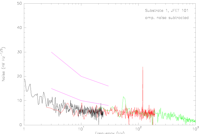
The median amplifier noise is 4.4, 3.9, and 3.7 nV Hz^-1/2 at 3, 10, and 30 Hz, and has been subtracted from the noise spectra.
During the first cooldown, 127 of 128 JFETs were functional; the drain wirebond on the nonfunctional device was accidentally omitted. The noise performance was marginal. In group A, 5 JFETs had noise in excess of the tight cutoff (allowance of 4), and 2 had noise in excess of the looser cutoff (allowance of 1). In group B, the number of noisy JFETs was 5 and 3 for the two cutoffs; C: 2 and 0, D: 3 and 1. Only groups C and D passed. We replaced the following JFETs: 101, 106, 206, 207, 215, 220, 221, 223, 231, 316, 329, 407, 423, and 427.
During the second cooldown, all 128 JFETs were functional. We remeasured the replaced devices, and the noise performance was well within specifications, with a median of 8.8, 4.9, and 4.0 nV Hz^-1/2 at 3, 10, and 30 Hz. There is only one device (404) which does not fall under the tight noise cutoff.
At 120 K, the JFET gain was 0.996+-0.001, and the source voltages were 0.543 to 0.587 V. These parameters are dependent on the operating current, which for our measurements is 18 microamps.
The noise data are available on-line:
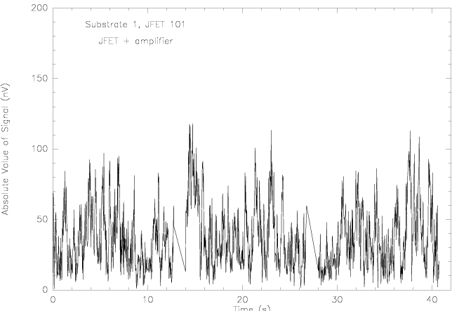
A caveat about the time records: due to the quirks of the spectrum analyzer, a true 'oscilloscope' mode is not available. Only the absolute value of the voltage as a function of time is available.
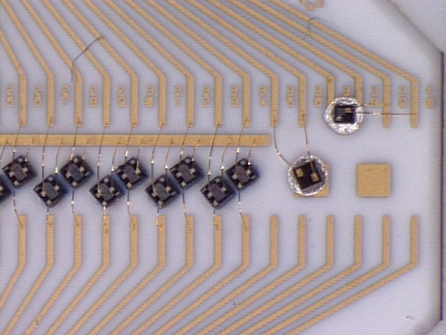
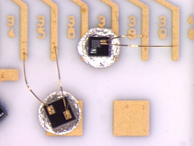
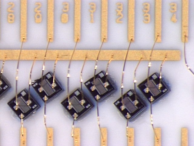
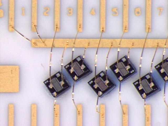
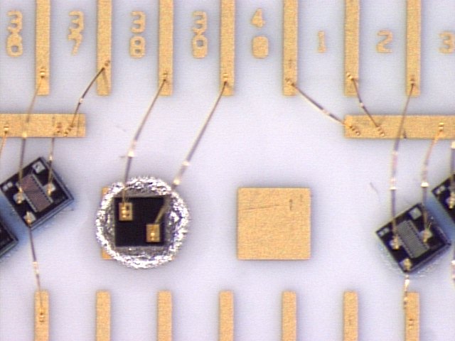
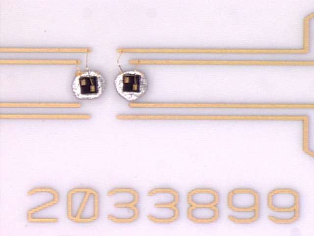
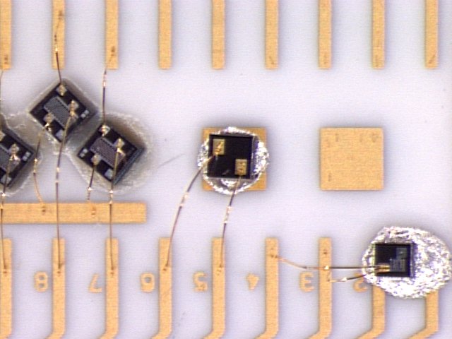
Figures. Photographs of components on assembled/wire bonded substrate
#1. For the diodes, conductive epoxy is used to make the electrical
connection from the collector to the gold traces.
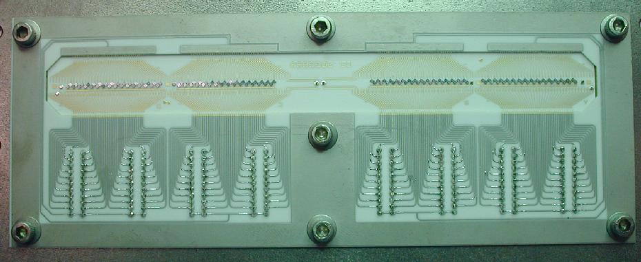
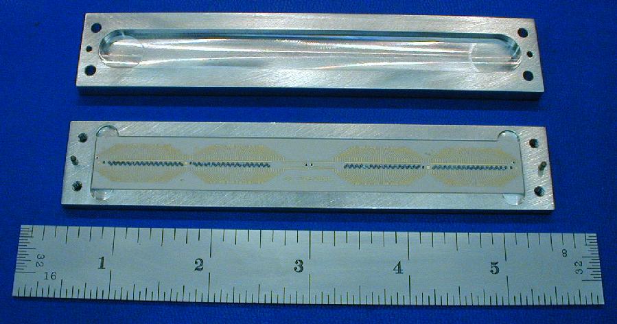
Figure. JFET substrate #1, post wire bonding, installed in test
fixture. The test fixture has wire bond interfaces to the warm board, and
connectors on the underside to interface with the amplifier electronics.
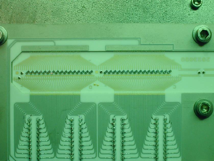
Figure. Closeup view of interface fixture.
PLAN: Substrate #1 will be electronically characterized at Caltech at ~120 K. Assuming no unanticipated problems, we will then send the warm board to Goddard for evaluation and integration with the JFET drawer.
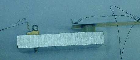
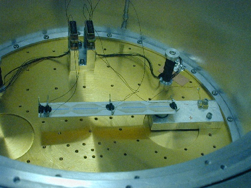
Figure. Three diodes were glued to the warm board -- 'C' at the
end near the G10 tube, 'A' at the far end, and 'B' in the middle. The heater
resistor was located at the far end near diode 'A'. This setup provides a
worst case for the warm board, with all of the heating at one end and all of
the cooling at the other.
temperature   time A    time B    time C
-----------  --------  --------  --------
    77 K      4.1 min   4.4 min   4.6 min
   120 K     21        25        25
The integrated heat capacity of the assembly from 4 K to 77 K is 13 Joules, and
the integrated heat capacity from 4 K to 120 K is 75 Joules.
The waiting time of 25 minutes at the reasonable power level of 50 mW is acceptable in our opinion.
Diode  Temperature
-----  -----------
  A       78.1 K
  B       77.7 K
  C       77.9 K
base       4.8 K
The temperature gradient across the board is less than 0.5 K.
Diode  Temperature
-----  -----------
  A      120   K
  B      117   K
  C      117   K
base       5.5 K
The temperature gradient across the board is no greater than 3 K. However, this is a large amount of power.
For a G10 thermal conductivity of 0.3 W/m/K, and two 0.05" glue lines, we would expect a power of ~35 mW to be required to warm the board to 120 K. This is consistent with the measurement.