Characteristics of SHARC II/HAWC JFETs measured by D. Dowell
Darren Dowell -- (626)395-6675 (office), -2600 (lab), 796-8806 (FAX)
Last modified Monday, 14-Feb-2000 10:41 PDT
cdd@submm.caltech.edu
Noise Requirements
SHARC2 JFET specification summary:
- en <= 15 nV/sqrt(Hz) at 3 Hz
- en <= 10 nV/sqrt(Hz) at 30 Hz, preferably <= 5 nV/sqrt(Hz)
- in <= 0.1 fA/sqrt(Hz) at f >= 3 Hz
- For the 32 JFETs reading out one row, Vs (Vg = 0; Ids = 25 uA) has a
maximum range of 50 mV.
- Yield > 90%
HAWC JFET specification summary: *******
InterFET NJ132L
I have looked at the noise and DC characteristics of several dozen InterFET
NJ132L devices at cold temperatures. Assuming a room temperature sorting by
DC parameters,
the NJ132L's meet the requirements for SHARC2 with > 80% reliability. With
elimination of devices with low room temperature transconductance, the
yield may be more like 90%.
Here is a Postscript document I sent to Yerkes in
February 1999 in recommendation of the NJ132L's.
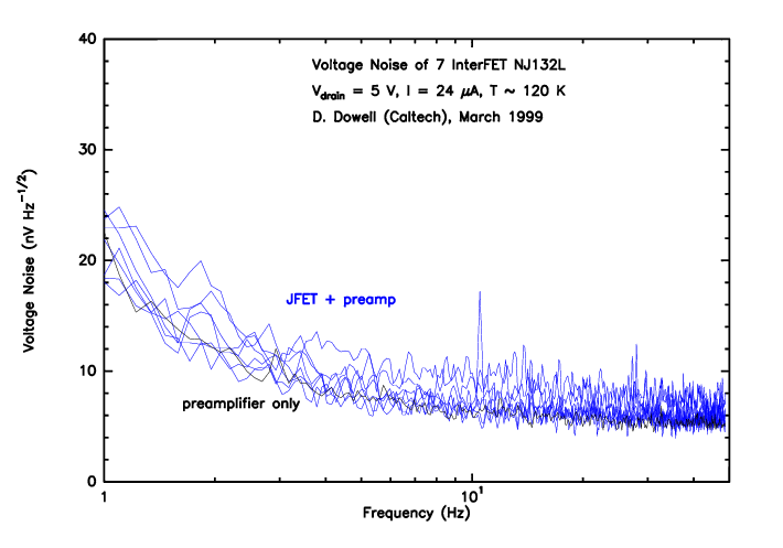
More detailed tests of 9 additional dies
occurred in March 1999. A voltage noise summary follows:
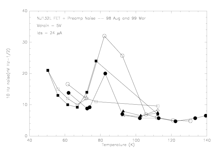
The operating temperature for the NJ132L should be >= 110K, although
operation at 65K is tempting:
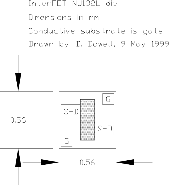
Here is the layout of a die:
Here is a scanned image of the InterFET NJ132L
data sheet in Postscript format.
NJ132L Selection at Caltech
We have 1000 dies, dated 4-14-99, lot #903934-6. They were purchased
for $2.11 each.
PUT INFORMATION ABOUT SELECTION PROCESS HERE.
GSFC JFETs -- November 1999
Four JFET samples were obtained from N. Das in Oct. 1999, packaged in
transistor caps labeled '4' and '5'.
For the DC measurements, the (common) drain voltage was 5 V. The gates were
grounded. The 'source voltage' is measured with a 500 kohm resistor to a
-12 V supply. The 'output impedance' is transconductance^-1, measured for
I ~ 30 microA.
temperature     JFET source voltages (V)     JFET output impedance (ohm)
-----------     ------------------------     ---------------------------
300 K           2.16, 1.73, 1.75, 1.78       3069, 2576, 2601, 2581
150             1.99, 1.53, 1.55, 1.58       2269, 1734, 1761, 1743
130             1.95, 1.49, 1.52, 1.54       2187, 1664, 1691, 1702
115             1.93, 1.47, 1.49, 1.52       2176, 1667, 1694, 1691
 95             1.89, 1.43, 1.46, 1.48       2241, 1732, 1759, 1740
 88             1.86, 1.41, 1.43, 1.46       2347, 1810, 1822, 1833
 77             1.82, 1.37, 1.39, 1.42       2545, 2011, 2023, 2019
The minimum output impedance (maximum transconductance) occurs at ~120 K.
The voltage noise was measured with the Yerkes 16-channel preamplifier and
a Stanford Research spectrum analyzer. The common drain voltage was 5 V, the
gates were grounded, and the source terminals were connected to a -12 V
supply through a 500 kohm resistor. The operating current was ~25 microA.
The first JFET was not measured due to a problem in the preamplifier channel
1.
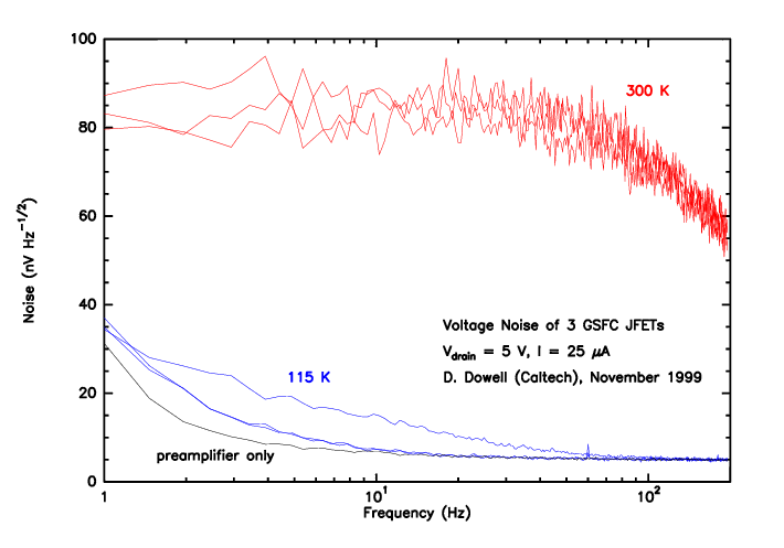
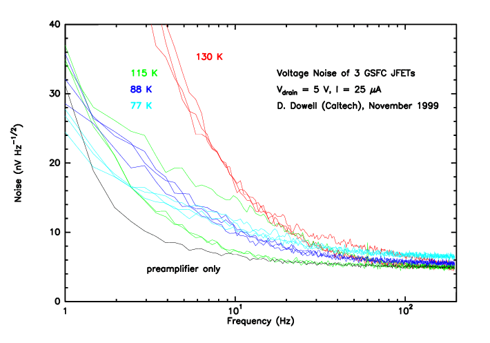
At room temperature, the JFETs are noisy (~85 nV Hz^-1/2). The optimum
noise performance occurs at ~90 K, for which the intrinsic voltage
noise is approximately:
- 3 Hz: ~15 nV Hz^-1/2
- 10 Hz: ~ 9 nV Hz^-1/2
- 30 Hz: ~ 5 nV Hz^-1/2
- 100 Hz: ~ 3 nV Hz^-1/2
This is reasonably good performance. However, the median performance of an
InterFET under the same conditions is as good or better, and the output
impedance is lower by nearly a factor of 2.
SHARC2 Readout
SHARC2 has requirements on both noise and the DC parameters. The
requirements are based on the expected detector
noise and the readout
scheme. The primary readout scheme calls for pairs of 2 pixels from a
32-detector row to be differenced in hardware, similar to the successful
SuZIE instrument at the Caltech Submillimeter Observatory (CSO):
The AD624 is operated with a gain of 100 (AC and DC). To keep the DC
output in comfortable range of the supplies, the JFET source voltages need to be
matched to within 50 mV, which would result in an output of 5V. Matching
the source voltages may also have the advantage of matching the JFET gain.
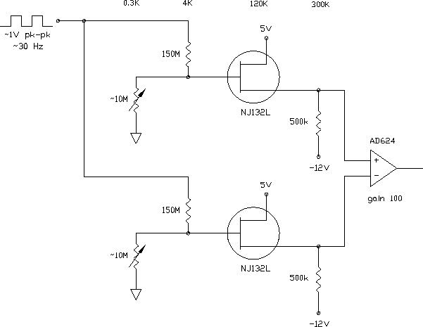
An AC-biased readout scheme has been tested at Caltech; here is a picture of
our prototype circuit to read 4 pixels:
One final note about the AC-biased readout -- the detector impedance should
be on the low side (5-10 Mohms) to minimize the glitches at the transition
of the bias voltage. This makes more stringent requirements on the amplifier;
however, an advantage of relatively high modulation frequency (~30 Hz) is
gained.
In case the primary readout scheme fails for some reason (unmatched JFETs,
unmatched detectors, low detector yield, very high detector impedances, ...),
we will fall back to the traditional DC-biased readout,
although there will be significant disadvantages to the instrument
capability:
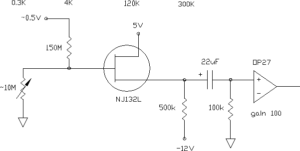
For a DC-biased SHARC2 readout, the requirement is for low noise (<= 15 nV/
sqrt(Hz)) at
3 Hz, because this is approximately the maximum signal modulation frequency
at the CSO. A large (10-40 Mohm) detector impedance can help beat the
amplifier noise.
Go to SHARC II home page...