HFSS Simulations with a 50 µm Quartz (Er=3.78) Substrate


Electric-field in 4 section RF choke

HFSS Simulations Results

    Quartz based E-probe inside waveguide  
  • 3-D rendering of probe  
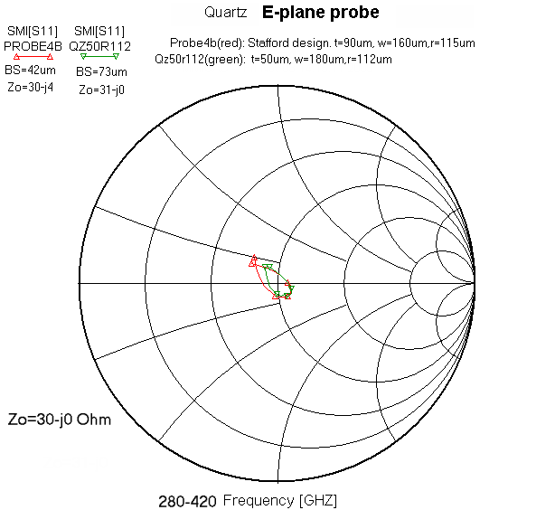
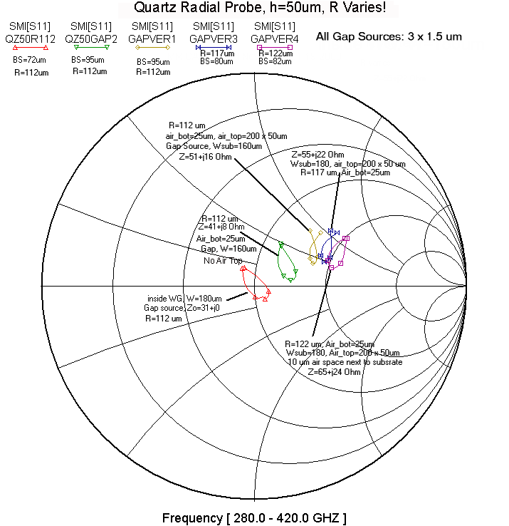
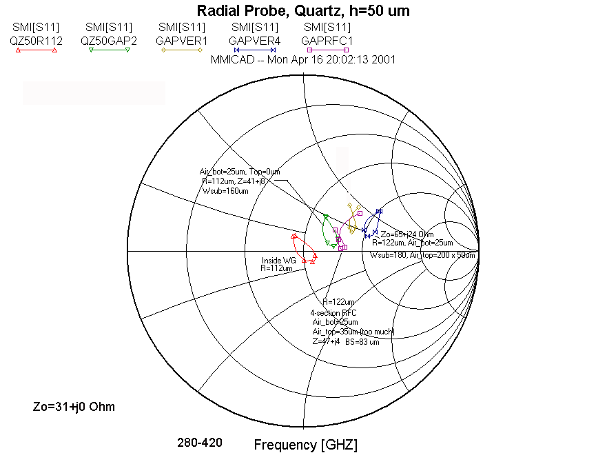
  • Impedance (Smith Chart) of 90 µm substrate height (Stafford Withington, Univ. Cambridge UK) and
        the 50 µm thick substrate probe for use at the Caltech Submillimeter Observatory (CSO)  
  • Effect of changing the Radius of the probe
        Comparison of Silicon and Quartz E-plane probes  
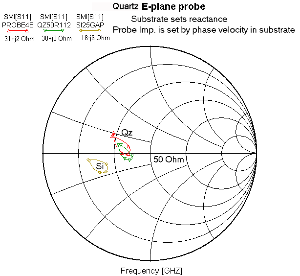
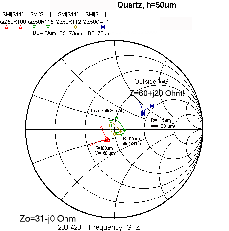
  • Comparison of Silicon and Quartz Radial probe impedance
        The original (Stafford Withington, Univ. Cambridge UK) design was on 90 µm substrate and has more reactance than the
        thinner 50 µm CSO probe design. The fundamental probe impedance is too a large extend set by the substrate's phase velocity.
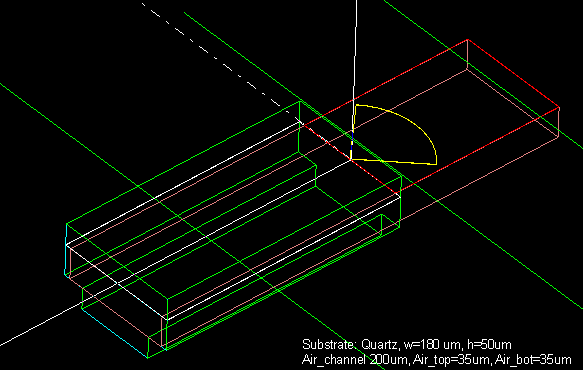
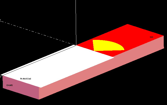
         Effect of breaking WG wall (perfect Gnd)  
  • 3-D wireframe of probe and substrate extending outwards from waveguide,  
  • 3-D rendering of probe and substrate extending outwards from waveguide,  
  • Impedance (Smith Chart) showing a large effect when radial probe is taken out of the waveguide:
        The WG opening size surrounding the probe has a large effect on the probe impedance. As shall be seen,
         putting in a RF Choke instead of a perfect ground reduces the real and imaginary parts of the probe impedance.  
  • Effect of using a different size of Gap source (minimal)  
  • Summary of Probe's sensitivity to radius and WG opening geometry
         Introduction of RF Choke (instead of a perfect Ground)  
  • 3-D wireframe of probe and substrate extending outwards from waveguide,  
  • Impedance (Smith Chart) showing the effect of introducing an RF Choke
     
    |Receiver index | HFSS Homepage | Scalemodel | Silicon-Probe design | CSO Homepage |
            Web Page created and last updated on April 16, 2001, by: Jacob W. Kooi