Pop-Up Detector Test Report
26 April 2000 11AM
C. Darren Dowell
Caltech, Mail Code 320-47
Pasadena, CA 91125
(626)395-6610 (office)
(626)395-2600 (lab)
(626)796-8806 (FAX)
cdd@submm.caltech.edu
Abstract
Measurements of semiconducting pop-up bolometers were performed at Caltech
in April 2000. We report the resistance vs. temperature and the thermal
characteristics of the measured samples. The desired SHARCII and HAWC
parameters were bracketed with the measured samples, and we make
recommendations for the bolometer designs for the two instruments.
Acknowledgments
Walter Collins (Caltech), Mino Freund (Goddard), Matt Gardner (Caltech), and
Jeff Groseth (Caltech) helped considerably with preparing the test
components and in performing the measurements. Attila Kovacs (Caltech)
wrote the software to solve for bolometer parameters from measured data.
Christine Allen (Goddard) provided the bolometer samples and advice for
handling them. Harvey Moseley (Goddard) provided guidance through the
testing period.
Outline
- Measurement apparatus
- Bolometer design
- Thermistor results
- Results for 5327 G0 test array
- Results for 5347 G0 test array
- Fitted parameters
- White noise
- Time constants
- Results for 5347 thermistor test array
- General conclusions
- Recommendation for SHARCII bolometer design
- Recommendation for HAWC bolometer design
Implant and bolometer samples were tested in the SHARCII cryostat, which
contains a 3He refrigerator enclosed in a L4He-cooled
radiation shield. For most measurements, the main L4He reservoir
was pumped down to 1.5 K so that the device substrate reached temperatures as
low as 0.325 K.


Figure 1. Interface substrate. The 3-element implant
screening devices
were GE varnished to the substrate, and the 32-element bolometer arrays were
clipped to the substrate. Gold wedge bonds provided electrical connection
between the devices, load resistors, and substrate. Surface-mount connectors
were initially
used to interface with the cryostat wiring. However, they were replaced
with directly soldered wires for later measurements. The ceramic substrate
was partially enclosed in an INVAR box. A sheet of gold leaf and the force
of ~6 screws were used to thermally connect the INVAR and ceramic.


Figure 2. Device suspension and shielding. The ceramic/
INVAR package was suspended from the L4He coldplate with 3-4
fiberglass tubes
with A/L = 0.014-0.018 cm. The package was heat sunk to the fridge through an
annealed OFHC copper strap with A/L = 0.014 cm. A calibrated LakeShore GRT
was attached to the ceramic substrate with a screw and gold leaf, approximately
5 cm from the detectors. The package was shielded by a secondary
L4He
enclosure with blackened walls. With this configuration, the coldest observed
GRT measurement for the detector package was 0.325 K, during which the
L4He bath was at 1.5 K and the fridge was at 0.291 K.

Figure 3. Additional implant screening hardware. In order
to confirm the implant resistances, the 3-element devices in the Goddard-
selected ceramic package were attached to a copper block and installed directly
on the SHARC II fridge coldhead or in a separate L4He cryostat
(the purple 'Barney' Dewar).
All wires going into the Dewar pass through one or two RFI-filtered
connectors, which contain 4 nF capacitors from each pin to the Dewar wall.
***Thermal properties of detector package, gold bonds, and silicon frame.
The silicon frame has a thickness of 300 microns. In the various directions
of heat flow, the relevant A/L is from approximately 0.0015 cm to 26 cm. For
a 0.3 K thermal conductivity of ***
The wirebonds were 0.001 inch diameter 99.99% gold. With 64 each 3 mm long
wire bonds (total A/L=0.001 cm), and assuming a 0.3 K thermal conductivity of
0.1 W/cm/K (Touloukian et al. 1970), the effective G of the wirebonds was
100 microW/K. We have
ignored unknown boundary thermal resistance, which will reduce the effective
G.
The ceramic substrate...
The heat strap also limits the cooling of the detector wafer. During the
cooldowns reported here, the fridge/heat strap combination was observed to
have an effective G of 80 microW/K at the coldest temperatures.
For a 0.5 V bias across the 30 Mohm load resistors (and detectors), the
dissipated power can be at most 0.5 microW.
Three types of bolometer arrays were manufactured for the detector measurements:
- 3-element implant screening dies with all membrane (high G) devices
- 32-element G0 variety packs with a range of thermal designs
(HGUNITs)
- 32-element thermistor variety packs with a range of thermistor designs
(THUNITs)

Table 1. Recipes for bolometers on G0 test
arrays.

Table 2. Recipes for bolometers on thermistor test arrays.

Table 3. Implant doses. Higher net density means greater
implant dose, which means lower cold resistance. Wafers 5347 and 5327 are
of interest for SHARCII and HAWC.
The first part of the detector measurement program was to screen five wafers
for desired resistance at cold temperatures. Three-element membrane devices
were measured in three configurations -- GE varnished to the Caltech ceramic
interface board, packaged in the Goddard ceramic carrier on a copper block
in the purple L4He dewar, and in the Goddard carrier/copper block
on the SHARCII coldhead.
Resistance measurements were made with a Keithley 616 Digital Electrometer
borrowed from Goddard that allows current excitations from 1 pA to 1 microA
stepped by factors of 10. The reported measurements were made with the
highest current setting which does not cause significant self heating. The
criterion was to allow no more than a 5% effect on the observed resistance.
SHARCII Dewar, Large Ceramic Board

Figure 4. Resistance measurements for 3-element membrane
devices on Caltech ceramic board. The SHARCII target curve is
T0 = XXX, R0 = YYY (REFERENCE),
and the HAWC target is
T0 = 30 K, R0 = 700 ohm (Moseley 1999).

Figure 5. Resistance measurements plotted in units which
give linear fits.
A fit to the data with model
R = R0 exp[(T/T0)1/2] yields:
Label   ND   R0 (ohms)  T0 (K)
-----  ----  ---------  ------
5250a  0.6     2570      81.8
5250b  0.6     3880      74.6
5327   0.7     1750      48.9
5347   0.75    2090      25.7
Table X. CAPTION... Checked these.
SHARCII Dewar, Small Ceramic Package on Coldhead
Purple Dewar, Small Ceramic Package
Three-element dies were tested using the Goddard-provided ceramic packages
attached 'upside down' to a copper block in order to shield the devices
from radiation. Resistances were measured with the Keithley 616 electrometer.
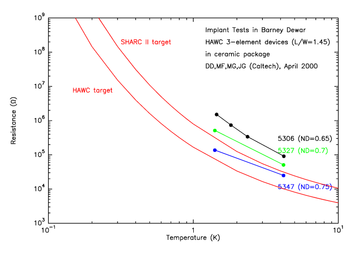
 Figure X. CAPTION... Checked these.
A fit to the data from the purple Dewar experiment only yields:
Label   ND   R0 (ohms)  T0 (K)
-----  ----  ---------  ------
5306   0.65    1670      67.3
5327   0.7     2100      42.7
5347   0.75    2380      23.2
Table X. CAPTION... Checked these.
Purple Dewar, small ceramic package
***Circuit. JFET gain.
The bolometer parameters are derived from a minimization procedure in which
the measured I's and V's are compared with a best-fit four-parameter model.
The model is:
- R = R0 exp[(T/T0)1/2]
- G = G0 Tbeta
See Mather (1982) for further details of the model.
Table X. Four-parameter fits for G0 bolometer
array 5327 ***. The four parameters are R0, T0, G0, and beta.
All bolometers were wired with 30 Mohm nichrome load resistors from MSI. They
were measured with two separate cooldowns between which the routing of the 16
JFETs was changed.

Figure X. Sample IV curve for a single bolometer at
multiple temperatures. The filled circles are measured data, and the lines
are model fits with 4 free parameters.
G0 test array 5347 LH1
Data at 330, 440, 597, 742, 985, 4243 mK (pixels 1-16)
Data at 329, 448, 604, 744, 974, 4261 mK (pixels 17-32)
Updated 26 Apr 2000, 10:30 PDT

R = R0 exp(sqrt(T0/T))
G = G0 T^beta

                        R*     R
          R0    T0    0.3 K  0.5 K   G0=G(1 K)          G(0.3 K)*  G(0.5 K)
bol/grp  ohms    K    Mohms  Mohms  W/K^(beta+1)  beta     W/K       W/K
-------  ----  -----  -----  -----  ------------  ----  ---------  ---------
01 mem.  1844  26.25   21.3   2.59    23.3 e-9    0.55  12.1  e-9  15.9  e-9
02 TH.1  1290  25.58   13.2            1.07e-9    1.32
03 TH.1  1365  25.51   13.8   1.73     1.20e-9    1.19   0.29 e-9   0.53 e-9
04 TH.1  1401  25.31   13.7            0.94e-9    1.15
05 HG3D  1953  26.94   25.5           24.4 e-9    1.97
06 HG3D  1956  27.16   26.5   3.11    24.1 e-9    1.96   2.28 e-9   6.19 e-9
07 HG3D  2147  27.11   28.9           19.4 e-9    1.77
08 HG3C  2127  26.93   27.7            2.24e-9    1.20
09 HG3C  1844  27.58   26.9   3.10     2.66e-9    1.38   0.51 e-9   1.02 e-9
10 HG3C  1898  27.05   25.2            2.61e-9    1.35
11 HG3B  1934  28.40   32.5           24.2 e-9    2.03
12 HG3B  1908  28.51   32.7   3.63    25.1 e-9    2.06   2.10 e-9   6.02 e-9
13 HG3B  1869  28.76   33.4           27.8 e-9    2.14
14 HG3A  1840  28.67   32.4            4.08e-9    1.44
15 HG3A  1951  28.41   32.9   3.66     3.80e-9    1.42   0.69 e-9   1.42 e-9
16 HG3A  1924  28.37   32.2            3.89e-9    1.41
17 HG2D  1893  28.73   33.7           38.4 e-9    2.63
18 HG2D  1899  28.90   34.8   3.80    38.7 e-9    2.66   1.57 e-9   6.12 e-9
19 HG2D  1981  28.82   35.8           36.7 e-9    2.65
20 HG2C  2025  28.51   34.7            1.17e-9    1.35
21 HG2C  1839  28.97   34.1   3.72     1.31e-9    1.43   0.23 e-9   0.49 e-9
22 HG2C  1920  28.91   35.2            1.26e-9    1.40
23 HG2B  1957  29.47   39.4            1.21e-9    1.37
24 HG2B  2038  29.15   38.9   4.22     1.17e-9    1.34   0.23 e-9   0.46 e-9
25 HG2B  1929  29.84   41.4            1.25e-9    1.40
26 HG2A  1871  30.40   44.0           42.4 e-9    2.76
27 HG2A  2019  29.93   44.0   4.63    37.3 e-9    2.62   1.59 e-9   6.07 e-9
28 HG2A  1952  30.41   46.0           40.0 e-9    2.69
29 HG1A  1836  31.16   49.0           20.0 e-9    2.74
30 HG1A  1788  31.95   54.2   5.30    20.7 e-9    2.80   0.71 e-9   2.97 e-9
31 HG1A  1927  31.34   52.9           18.1 e-9    2.68
32 mem.  1814  32.12   56.5   5.49    72.9 e-9    1.58  10.9  e-9  24.4  e-9

* extrapolation
Table X. Four-parameter fits for G0 bolometer
array 5347 LH1.
***Interpretation...
Resistance Gradient
The cold resistance goes from high at bolometer 32 to low at bolometer 1. In
order to confirm this situation, a few bolometers were measured individually
with an electrometer. The 0.327 K resistance measured in the linear portion
of the IV curve is tabluated below:
           Electrometer  Table X Fit
            Resistance   Resistance
Bolometer      Mohm         Mohm
---------  ------------  -----------
    1          15.6         14.4
    9          19           18.0
   12          23           21.7
   15          22           21.8
   24          28           25.7
   32          36.4         36.6
*** Do calculation for power required to warm bolometer 1 up from resistance
of bolometer 32.
***Circuit.
***Circuit.
For the time constant measurements, the bolometers were driven using a bias
waveform with a square profile switching between two positive levels 8 mV
apart. The output of the JFET was sent to an
SR560 preamplifier with a gain of 100 and then to an oscilloscope. DC coupling
was used on both instruments; a DC level from a power supply was subtracted to
bring the signal on scale. Low-pass filtering was applied with the SR560,
but the cutoff frequency (typically 3 kHz) was chosen so that only high
frequency noise was eliminated and the shape of the waveform was preserved.
Additional filtering of the bolometer waveform was caused by the bias waveform
filtering (cutoff frequency at 6800 Hz) and the RFI connectors (cutoff
frequency at 20 kHz, assuming a 1000 ohm JFET output impedance). However,
these cutoff frequencies are high enough to be irrelevant.

Figure ***. Typical oscilloscope trace during time constant
measurement. Shown is the output of the JFET for bolometer 24 of the 5347
G0 test array, multiplied by a gain of 100. The bias frequency was 8 Hz, and
the settling time was 3.6 msec.
The overshoot is caused by the high-frequency impedance of the bolometer
being larger than the low-frequency impedance (Mather 1982). Stated another
way, the dynamic circuit model of a bolometer contains an effective inductance,
which creates a voltage spike at the transition of the bias.
Our interpretation is that the overshoot spike is rolled off (i.e., not
instantaneous) by parasitic capacitance (time constant Rbolometer
x Cparasitic). The settling of the voltage following the bias
transition is the true detector time constant (taue in the
notation of Mather 1982).
*** Reconsider overshoot tau -- note large t(o.s.) for low G (bol. 24).
For the measured quantities, we looked at the transition caused by the positive
change in the bias. We recorded:
- V(step) -- the voltage from the initial (flat) voltage to the final (flat)
voltage.
- V(o.s.) -- the voltage from the final (flat) voltage to the peak
voltage. ('o.s.' for overshoot.)
- t(o.s.) -- the time from the beginning of the transition to the peak
voltage.
- t(settle) -- the time from the peak to when the voltage has slewed 63%
of the way to the final voltage. The true time constant taue.
In the table below, voltages are referred to JFET output, before the
preamplification. The calculated G and T are the estimates from the IV curve
fits.
                                                     calc.   observ.
            bias  calc G  calc T  V(o.s.)  t(o.s.)  V(step)  V(step)  t(settle)
bol.  grp.   mV    nw/K      K       mV      msec      mV       mV       msec
----  ----  ----  ------  ------  -------  -------  -------  -------  ---------
  9    3C    25     0.59   0.34     0.12     2.2      2.9      2.7       1.5
  9    3C    49*    0.64   0.36     0.42     1.1      1.4      1.4       1.6
  9    3C    98     0.76   0.40     0.70     0.52     0.34     0.40      1.2
  9    3C   196     0.98   0.48     0.61     0.28     0.02     0.06      0.71

 15    3A    39     0.84   0.34     0.19     1.8      2.2      2.2       1.6
 15    3A    78?*   0.95   0.38     2.8?     0.92     0.90     6.6?      1.1
 15    3A   157     1.20   0.44     0.69     0.31     0.12     0.18      0.61
 15    3A   314     1.60   0.54     0.47     0.24    -0.02     0.05      0.31

 18    2D    49     2.1    0.34     N.A.     N.A.     2.7      2.6       0.38
 18    2D    98*    2.5    0.36     0.20     0.8      1.5      1.5       0.68
 18    2D   196     3.6    0.41     0.46     0.31     0.45     0.53      0.36
 18    2D   392     5.6    0.48     0.34     0.22     0.12     0.22      0.16

 24    2B    20     0.28   0.34     0.39     2.4      2.6      2.7       4.5
 24    2B    39*    0.31   0.37     1.1      1.3      1.2      1.1       3.6
 24    2B    78     0.38   0.43     1.2      0.6      0.17     0.11      2.3
 24    2B   157     0.50   0.53     0.74     0.4     -0.03    -0.13      1.3

* optimum bias for NEP
? apparent errors in measurement, probably bias amplitude setting
Fitted Parameters
Thermistor test array 5347 RH7
Data at 330, 451, 610, 755, 971, 4190 mK
Updated 28 Apr 2000, 09:45 PDT

R = R0 exp(sqrt(T0/T))
G = G0 T^beta

                        R*     R
          R0    T0    0.3 K  0.5 K   G0=G(1 K)          G(0.3 K)*  G(0.5 K)
bol/grp  ohms    K    Mohms  Mohms  W/K^(beta+1)  beta     W/K       W/K
-------  ----  -----  -----  -----  ------------  ----  ---------  ---------
09 TH.1  1622  35.93   91.8            1.53e-9    1.67
10 TH.1  1658  35.50   87.9   7.57     1.52e-9    1.64   0.21 e-9   0.49 e-9
11 TH.1  1622  35.65   88.0            1.54e-9    1.69
12 TH.2  1800  34.29   79.1            1.42e-9    1.49
13 TH.2  1733  34.60   80.0            1.48e-9    1.53
14 TH.2  1726  34.57   79.3   7.05     1.49e-9    1.52   0.24 e-9   0.52 e-9
15 TH.2  1800  34.52   82.0            1.44e-9    1.51
16 TH.2  1802  34.41   80.7            1.44e-9    1.50
17 TH.3  1638  36.36   99.0            1.50e-9    1.57
18 TH.3  1668  36.19   98.2            1.49e-9    1.56
19 TH.3  1727  36.17  101     8.53     1.43e-9    1.56   0.22 e-9   0.48 e-9
20 TH.3  1693  36.09   98.2            1.46e-9    1.56
21 TH.3  1578  36.79  102              1.55e-9    1.62
22 TH.4  1096  33.11   40.0            1.42e-9    1.45
23 TH.4  1106  33.47   42.8   3.95     1.37e-9    1.42   0.25 e-9   0.51 e-9
24 TH.4  1108  33.03   40.0            1.37e-9    1.42

* extrapolation
Table X. Four-parameter fits for thermistor test
array 5347 RH7.
There is no strong resistance gradient as on the LH1 G0 device, as
shown in the following 0.330 K measurements acquired with an electrometer:
           Electrometer  Table X Fit
            Resistance   Resistance
Bolometer      Mohm         Mohm
---------  ------------  -----------
    1          15.6         14.4
    9          19           18.0
   12          23           21.7
   15          22           21.8
   24          28           25.7
   32          36.4         36.6
Low Frequency Noise

Figure X. CAPTION
Time Constants
Mather, J. C. 1982, Applied Optics 21, 1125, "Bolometer noise: nonequilibrium
theory"
Moseley, H. 1999, memo dated July 29, "Detector Design for HAWC"
**************************************************************
Thermal Conductance Variety Pack 5327 -- Results -- Apr. 12, 2000
Tests of G0 array LH5 with 5327 (ND=0.7) doping are complete. Bolometers
17-29 and 32 were wired in series with 150 Mohm SiCr load resistors. Bolometer
30 was shorted with no load resistor, and bolometer 31 was shorted with a load
resistor in the circuit. In all cases, the signals were routed to JFET gates.
Bolometers 1-16 were not wired. The array was clipped to the detector board
with beryllium-copper clips and gold wedge bonded.
Other changes to the system include using only 3 of 4 G10 support tubes, only
2 of 4 manganin cables, avoidance of the surface mount connectors on the
detector board, and using gold leaf between the INVAR base plate, detector
board, heat strap, and GRT interfaces.
Sample IV curves for all bolometers at a single temperature:
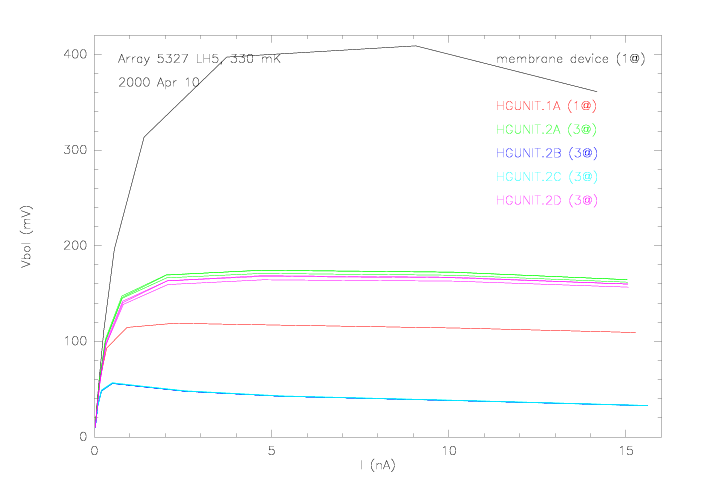
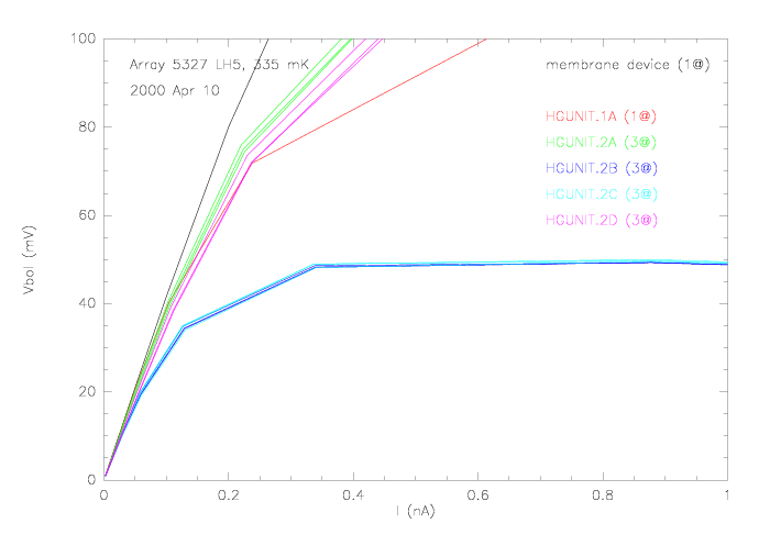
IV curves for a bolometer at multiple temperatures:

In the above graph, the filled circles are measured data, and the lines are
model fits with 4 free parameters.
The preliminary summary of bolometer parameters is as follows:
G0 test array 5327 LH5
Data at 328, 342, 389, 467, 651, 860, 962, 4127 mK
Updated 16 Apr 2000, 16:10 PDT

R = R0 exp(sqrt(T0/T))
G = G0 T^beta

            R0    T0     G0=G(1 K)          G(0.3 K)*  G(0.5 K)
bol./grp.  ohms    K    W/K^(beta+1)  beta     W/K       W/K
---------  ----  -----  ------------  ----  ---------  ---------
17  2D     1175  51.70    65.6 e-9    2.92
18  2D     1193  51.94    65.5 e-9    2.91   1.97 e-9   8.71 e-9
19  2D     1242  50.99    63.5 e-9    2.79
20  2C     1400  49.64     1.61e-9    1.24
21  2C     1271  51.22     1.70e-9    1.36   0.33 e-9   0.66 e-9
22  2C     1275  51.06     1.72e-9    1.35
23  2B     1354  50.20     1.65e-9    1.29
24  2B     1403  49.92     1.62e-9    1.28   0.35 e-9   0.67 e-9
25  2B     1304  50.94     1.67e-9    1.35
26  2A     1228  52.05    63.8 e-9    2.88
27  2A     1291  51.77    62.0 e-9    2.83   2.05 e-9   8.72 e-9
28  2A     1268  51.47    63.7 e-9    2.80
29  1A     1232  52.47    25.4 e-9    2.69   1.00 e-9   3.93 e-9
32  mem.   1243  52.25   128   e-9    2.40   7.12 e-9  24.3  e-9

* extrapolation; may not be accurate
Here is a
Postscript summary of the bolometer recipes to
associate with the group specification in the above table.