Last Updated May 5, 2001 by Jacob W. Kooi
J. Zmuidzinas, J. W. Kooi, , J. Kawamura, G. Chattopadhyay, B. Bumble, H. G. LeDuc, and J. A. Stern,
J.A. Stern, B. Bumble, H.G. LeDuc, J.W. Kooi, J. Zmuidzinas,
"Development of SIS mixers for 1 THz",
Proc. SPIE, vol. 3357, pp. 53-61
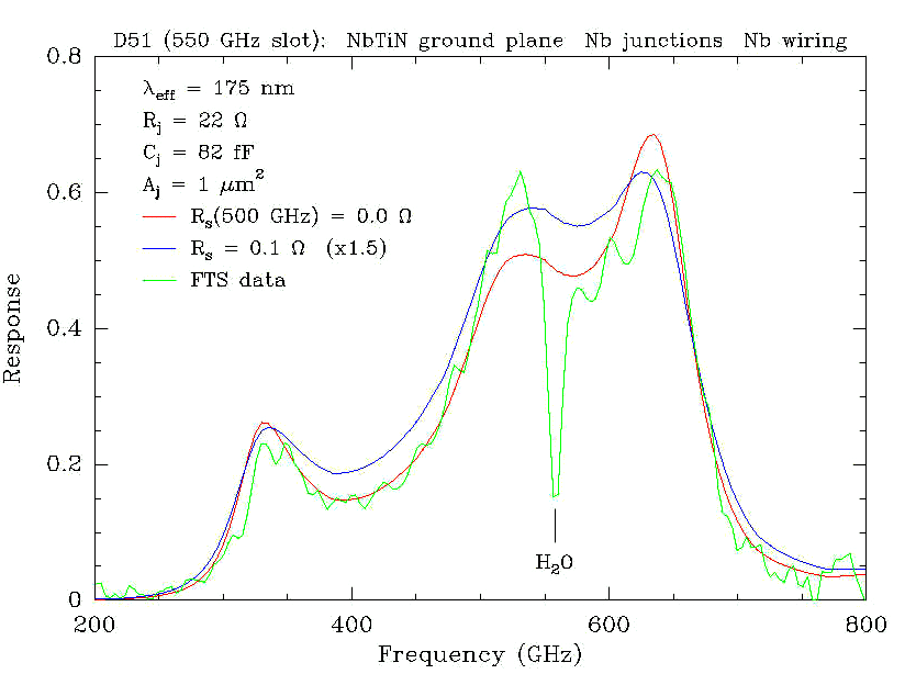
"Fabrication and DC-Characterization of NbTiN Based SIS Mixers for the Use betwen 600 and 1200 GHz".
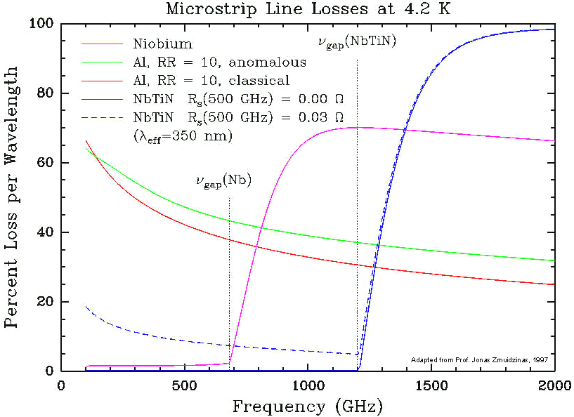
Calculated Losses for microstrip thin-film transmission line at 4.2 K.
The microstrip width is 5um and the SiO dielectric (Er=5.6) is
400 nm
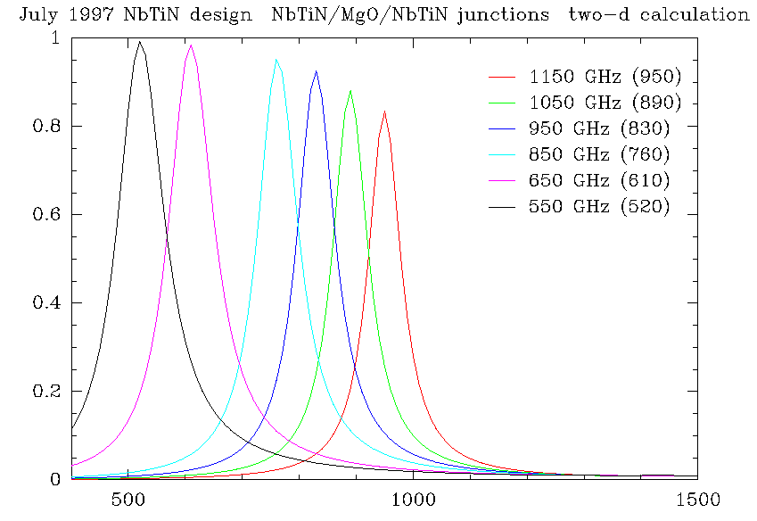
July 1997 mask with a full 2-Dimensional calculation of a NbTiN/MgO/NbTiN junction.
The first number is the design frequency, the number in
parenthesisis the actual 2_D simulated frequency.
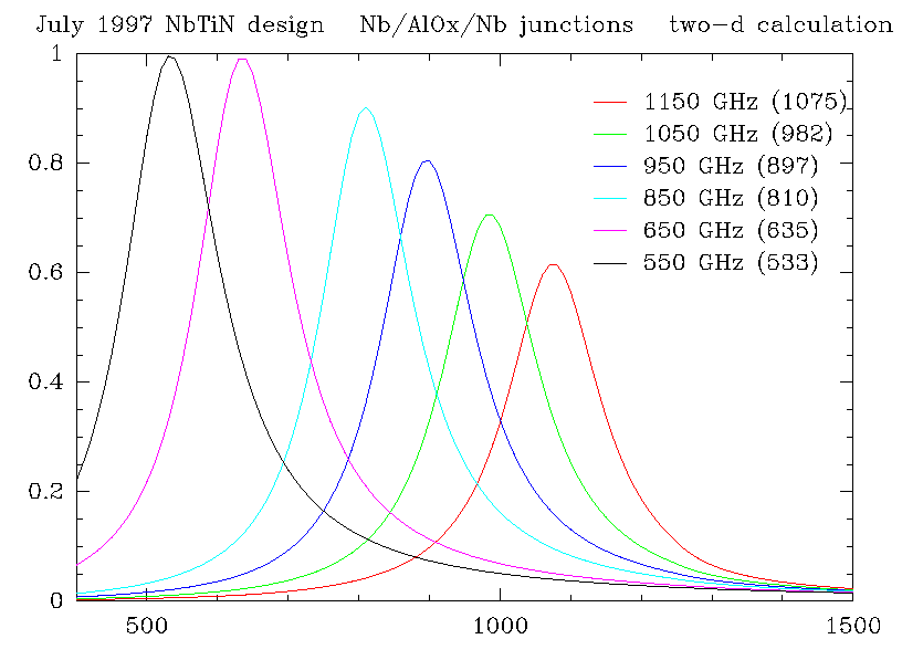
July 1997 mask with a full 2-Dimensional calculation of a Nb/AlOx/Nbjunction.
The first number is the design frequency, the number in
parenthesis is the actual 2_D simulated frequency.
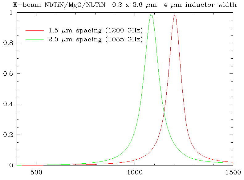
Below we present a full 2-Dimensional calculation with an E-beam
NbTiN/MgO/NbTiN 0.2um x 3.6um junction.
From the above it is quite aparent that a square 0.8um x 0.8um
junction is far from optimal.
(Same size junction as in the above
simulations).
Note the tremendous improvement in coupling efficiency and center
frequency, even at 1200 GHz!
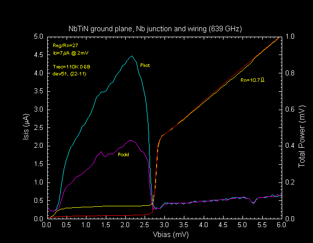
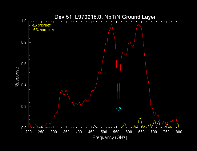
NbTiN Groundplane, Nb Wiring, Nb/AlOx/Nb Junction, Batch-L970218
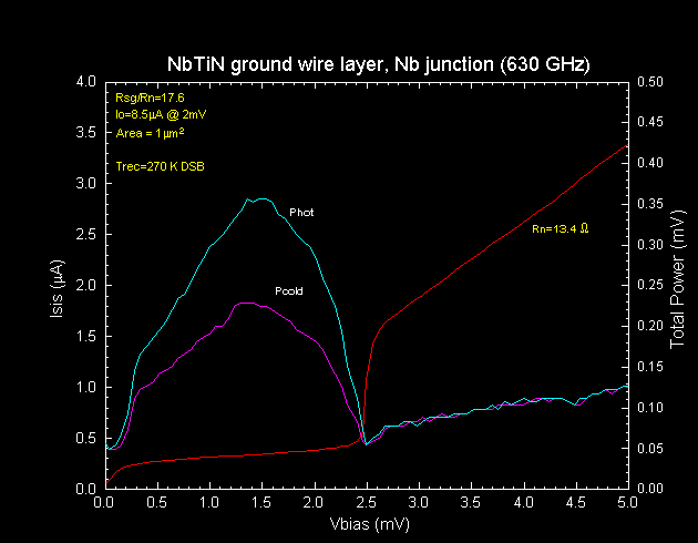
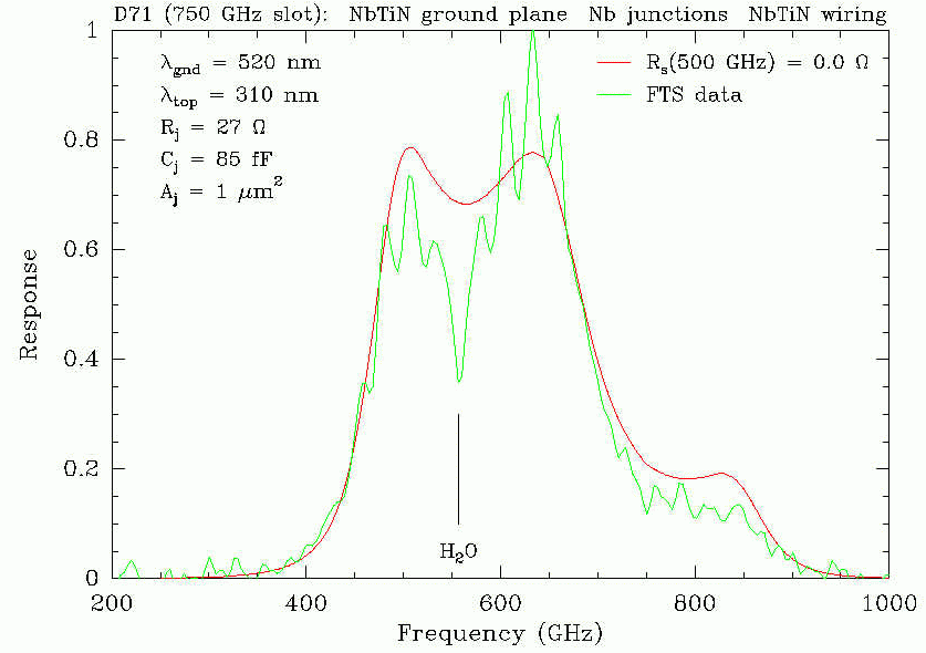
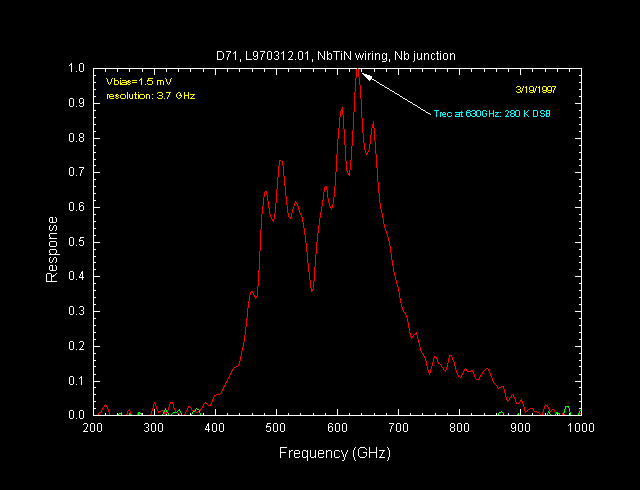
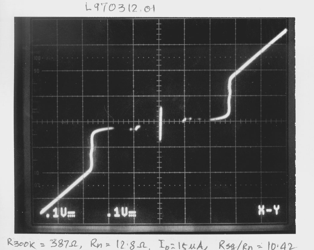
NbTiN Groundplane and Wiring, Nb/AlOx/Nb Junction, Batch-970312
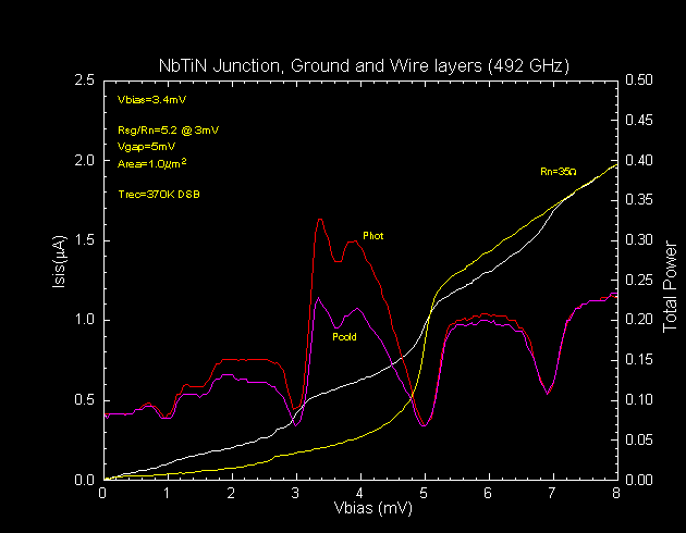
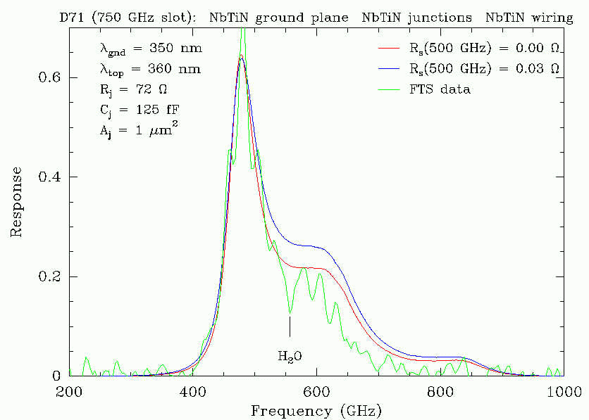
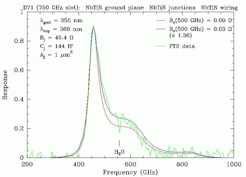
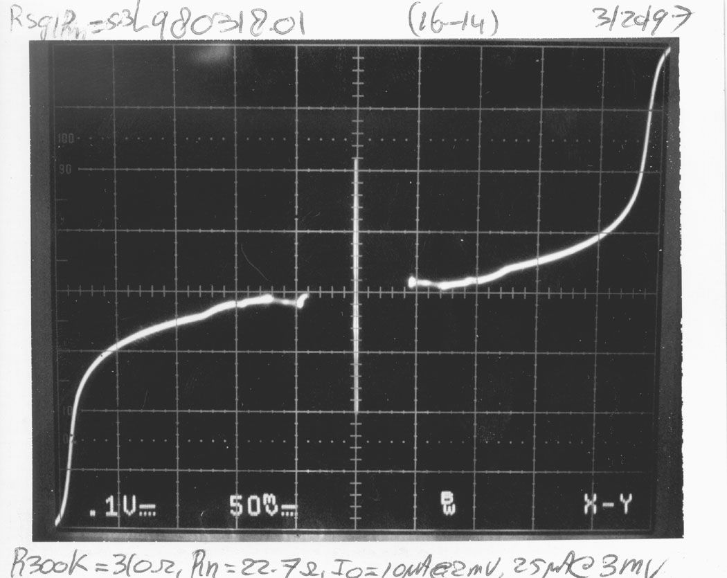
All NbTiN Device, MgO barrier. Batch-L970318
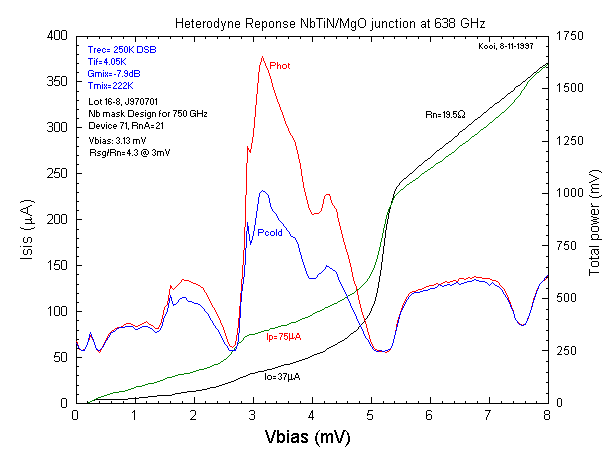
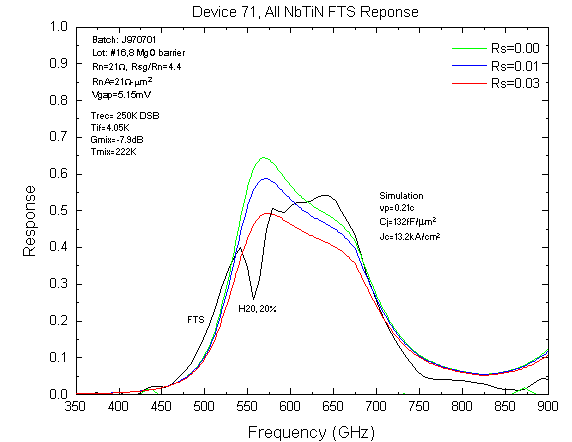
All NbTiN Device, MgO barrier. Batch-L970701
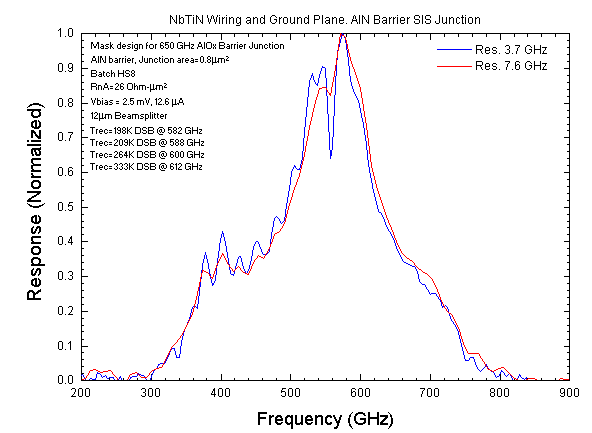
All NbTiN Wiring and Ground plane, NbTiN/AlN/Nb junction. Batch-L970811
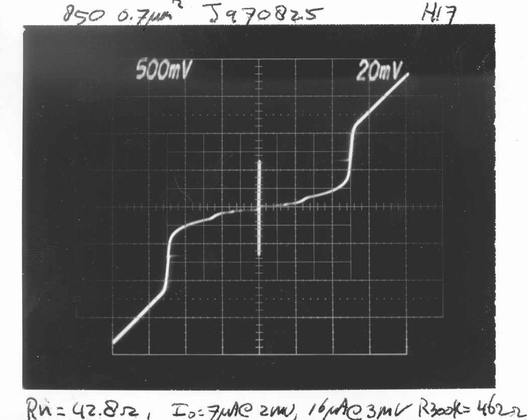
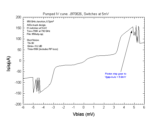
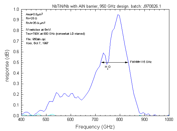
NbTiN Wiring and Ground plane(with a 1nm Nb layer), Nb/AlN/Nb junction. Batch-J970826
|
|Receiver Index | Beam Efficiencies | CSO Homepage | Tau | CSO Weather Page | Submm Physics | Caltech Astronomy | Web Page created and last updated on March 5, 2001, by: Jacob W. Kooi |