Test Report – Three-Bolometer Devices from
CSO Run 1
C. Darren Dowell (Caltech)
Version: 20 December 2000 (slight correction 20 September 2001)
Acknowledgments
Christine
Allen (NASA/GSFC) provided the bolometers.
Jeff Groseth (Caltech) glued and wirebonded the dies. Matt Gardner (Caltech) performed the
majority of the measurements.
Apparatus
Cryostat: Caltech Barney Dewar, which is IR Labs
HDL-10 with helium shield + Chase Research single-stage 3He
fridge. RFI filtered connectors with
1-4 nF capacitance.
Detector
holder: Up to 6 each 10 mm × 8 mm dies
attached with GE varnish to fiberglass PC board with gold-plated copper
traces. PC board screwed to Invar base
and covered with lid. Black paint on
inside of lid. Invar base attached with
screws and N grease to copper cradle, which is attached to fridge coldhead with
screws and N grease. Eight each gold
wirebonds (0.001”) provide electrical interface to each die. Calibrated Lakeshore G.R.T. attached to PC
board with screw and N grease.
Methods: Resistance measurements were taken at
approximately 2 K, 0.5 K, and 0.3 K, and in some cases 4 K and 0.35 K. 1) Current applied through bolometer in
series with one of four room temperature load resistors (310 MW, 20 MW, 1 MW, 0.1 MW) and measured
with Keithley 487 picoammeter. Total
voltage across load resistor/bolometer measured with HP 34401A multimeter. 2) Load resistors and JFETs inside Dewar
used during measurements. Bias voltage
switched at ~1 Hz from 0 to a range of voltages. Signal recorded with A/D and DSP. Bolometer V is obtained directly from amplitude, and bolometer I
is calculated from bias voltage, bolometer V, and load resistance.
Measurement
period: All measurements took place
between 2000 Nov. 10 and 2000 Dec. 6.
During
the Nov. 11 cooldown, we measured a bare bolometer on die 2041 T3 and one
coated with 1000 Å silver. At 0.282 K,
the resistances were 130 MW and 120 MW respectively.
During the Nov. 14 cooldown, we measured a bare bolometer on die 5311 T3
and one coated with 1000 Å silver. At
0.281 K, the resistances were 146 MW and 126 MW respectively.
Therefore, for the purposes of measurements of bolometers without absorbers, the detector
enclosure is dark and free of RFI heating.
During
the Nov. 24 cooldown, we measured a bare bolometer on die 2041 T2 and one
coated with a bismuth absorber. At
0.287 K, the resistances were 82 MW and 68 MW respectively. We
also measured a bare bolometer on die 5311 T2 and one coated with bismuth. At 0.287 K, the resistances were 35 MW and 29 MW
respectively. These results alone could
imply that a light leak is warming the bolometers with absorbers. However, this hypothesis does not result in
a good fit to the measurements including other temperatures. We suspect that the application of a metal
film to the back side of the bolometers results in a measurable decrease in
resistance, since this has now been observed in 4 out of 4 cases. (NEEDS UPDATING – EFFECT IS STILL THERE.)
Thermistor
Measurements
The
thermistor behavior is modeled as R = R0 exp(sqrt(D/T)). Sample
measurements from November 10-11 are shown in the figures below:
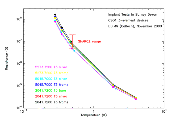
Figure
1 – Resistance vs. temperature for 3 dies.
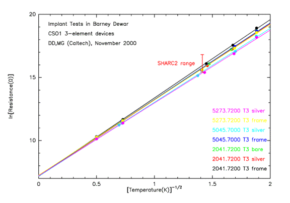
Figure
2 – Resistance vs. temperature shown in units which are expected to have a
linear relation.
Table 1 –
Resistance Measurements
|
Die |
Thermistor
Type |
Bol. Loc. |
Date |
Meth. |
D K |
R0 W |
R (0.5 K) MW |
|
5045.7000
T1 |
bare
bolometer |
mid |
Dec. 6 |
2 |
24.7 |
1602 |
1.80 |
|
5045.7000
T1 |
bare
bolometer |
right |
Dec. 6 |
2 |
24.7 |
1599 |
1.80 |
|
5045.7000
T2 |
bare
bolometer |
right |
Nov. 24 |
1 |
28.4 |
1412 |
2.65 |
|
5045.7000
T2 |
bare
bolometer |
right |
Nov. 26 |
2 |
26.0 |
1839 |
2.48 |
|
5045.7000
T3 |
bolometer w/
Ag |
right |
Nov. 11 |
1 |
34.4 |
1292 |
5.15 |
|
5045.7000
T4 |
w/
SiO/Bi/SiO |
left |
Dec. 19 |
2 |
38.3 |
1193 |
7.58 |
|
5045.7000
T4 |
bare
bolometer |
right |
Dec. 19 |
2 |
38.9 |
1161 |
7.90 |
|
5311.7000
T2 |
bolometer w/
Bi |
left |
Nov. 24 |
1 |
28.2 |
1442 |
2.64 |
|
5311.7000
T2 |
bolometer w/
Bi |
left |
Dec. 16 |
2 |
28.3 |
1513 |
2.81 |
|
5311.7000
T2 |
bare
bolometer |
right |
Nov. 24 |
1 |
29.4 |
1363 |
2.93 |
|
5311.7000
T2 |
bare
bolometer |
right |
Nov. 26 |
2 |
28.8 |
1508 |
2.98 |
|
5311.7000
T2 |
bare
bolometer |
right |
Dec. 16 |
2 |
29.4 |
1433 |
3.05 |
|
5311.7000
T3 |
bare
bolometer |
left |
Nov. 14 |
1 |
38.3 |
1212 |
7.67 |
|
5311.7000
T3 |
bolometer w/
Ag |
right |
Nov. 14 |
1 |
37.4 |
1187 |
6.73 |
|
5311.7000
T4 |
w/
SiO/Bi/SiO |
left |
Dec. 16 |
2 |
36.6 |
1302 |
6.80 |
|
5311.7000
T4 |
bare
bolometer |
right |
Dec. 16 |
2 |
37.4 |
1231 |
7.04 |
|
2041.7200
T2 |
bare
bolometer |
right |
Nov. 24 |
1 |
35.0 |
1239 |
5.33 |
|
2041.7200
T2 |
bare
bolometer |
right |
Nov. 26 |
2 |
34.1 |
1425 |
5.49 |
|
2041.7200
T2 |
bolometer w/
Bi |
left |
Nov. 24 |
1 |
33.6 |
1302 |
4.74 |
|
2041.7200
T3 |
bare
bolometer |
left |
Nov. 11 |
1 |
36.8 |
1327 |
7.03 |
|
2041.7200
T3 |
bolometer w/
Ag |
right |
Nov. 11 |
1 |
36.6 |
1283 |
6.68 |
|
5251.7200
T3 |
bolometer w/
Ag |
right |
Nov. 16 |
1 |
30.5 |
1441 |
3.57 |
|
5251.7200
T4 |
bare
bolometer |
mid |
Dec. 6 |
2 |
32.0 |
1560 |
4.63 |
|
5251.7200
T4 |
bare
bolometer |
right |
Dec. 6 |
2 |
33.2 |
1305 |
4.54 |
|
5273.7200
T1 |
w/ SiO/Bi/SiO |
left |
Dec. 19 |
2 |
25.0 |
1564 |
1.83 |
|
5273.7200
T1 |
bare
bolometer |
right |
Dec. 19 |
2 |
25.4 |
1503 |
1.87 |
|
5273.7200
T2 |
bare
bolometer |
mid |
Dec. 1 |
2 |
29.8 |
1492 |
3.37 |
|
5273.7200
T3 |
bolometer w/
Ag |
right |
Nov. 11 |
1 |
33.3 |
1342 |
4.72 |
|
5273.7200
T4 |
bare
bolometer |
mid |
Dec. 6 |
2 |
35.1 |
1398 |
6.12 |
|
5332.7200
T3 |
bolometer w/
Ag |
right |
Nov. 16 |
1 |
24.2 |
1525 |
1.60 |
|
5350.7200
T2 |
bare
bolometer |
mid |
Dec. 1 |
2 |
34.0 |
1317 |
4.99 |
|
5350.7200
T4 |
bolometer w/
Ag |
right |
Nov. 16 |
1 |
29.0 |
1523 |
3.08 |
|
2042.7375
T3 |
bolometer w/
Ag |
right |
Nov. 16 |
1 |
17.8 |
1764 |
0.69 |
|
5326.7375
T3 |
bolometer w/
Ag |
right |
Nov. 14 |
1 |
19.0 |
1690 |
0.80 |
|
5330.7375
T2 |
bare
bolometer |
mid |
Dec. 1 |
2 |
25.4 |
1525 |
1.89 |
|
5330.7375
T3 |
bolometer w/
Ag |
right |
Nov. 14 |
1 |
29.2 |
1362 |
2.85 |
|
|
|
|
|
|
|
|
|
|
5045.7000
T1 |
frame |
|
Dec. 6 |
2 |
25.3 |
1665 |
2.05 |
|
5045.7000
T2 |
frame |
|
Nov. 24 |
1 |
29.4 |
1425 |
3.05 |
|
5045.7000
T2 |
frame |
|
Nov. 26 |
2 |
28.6 |
1594 |
3.05 |
|
5045.7000
T3 |
frame |
|
Nov. 11 |
1 |
36.6 |
1345 |
7.02 |
|
5045.7000
T4 |
frame |
|
Dec. 19 |
2 |
39.7 |
1153 |
8.58 |
|
5311.7000
T2 |
frame |
|
Nov. 24 |
1 |
30.8 |
1370 |
3.49 |
|
5311.7000
T2 |
frame |
|
Nov. 26 |
2 |
30.4 |
1470 |
3.57 |
|
5311.7000
T2 |
frame |
|
Dec. 16 |
2 |
30.4 |
1402 |
3.43 |
|
5311.7000
T3 |
frame |
|
Nov. 14 |
1 |
40.7 |
1140 |
9.44 |
|
5311.7000
T4 |
frame |
|
Dec. 16 |
2 |
37.6 |
1232 |
7.20 |
|
2041.7200
T2 |
frame |
|
Nov. 24 |
1 |
35.7 |
1248 |
5.80 |
|
2041.7200
T2 |
frame |
|
Nov. 26 |
2 |
34.9 |
1368 |
5.84 |
|
2041.7200
T3 |
frame |
|
Nov. 11 |
1 |
38.5 |
1300 |
8.42 |
|
5251.7200
T3 |
frame |
|
Nov. 16 |
1 |
34.7 |
1342 |
5.58 |
|
5251.7200
T4 |
frame |
|
Dec. 6 |
2 |
34.0 |
1277 |
4.87 |
|
5273.7200
T1 |
frame |
|
Dec. 19 |
2 |
25.9 |
1511 |
2.01 |
|
5273.7200
T2 |
frame |
|
Dec. 1 |
2 |
31.9 |
1386 |
4.08 |
|
5273.7200
T3 |
frame |
|
Nov. 11 |
1 |
35.7 |
1405 |
6.54 |
|
5273.7200
T4 |
frame |
|
Dec. 6 |
2 |
35.9 |
1334 |
6.35 |
|
5332.7200
T3 |
frame |
|
Nov. 16 |
1 |
27.2 |
1567 |
2.50 |
|
5350.7200
T2 |
frame |
|
Dec. 1 |
2 |
35.2 |
1253 |
5.52 |
|
5350.7200
T4 |
frame |
|
Nov. 16 |
1 |
32.9 |
1375 |
4.57 |
|
2042.7375
T3 |
frame |
|
Nov. 16 |
1 |
19.0 |
1839 |
0.87 |
|
5326.7375
T3 |
frame |
|
Nov. 14 |
1 |
19.9 |
1765 |
0.98 |
|
5330.7375
T2 |
frame |
|
Dec. 1 |
2 |
27.0 |
1486 |
2.31 |
|
5330.7375
T3 |
frame |
|
Nov. 14 |
1 |
32.0 |
1321 |
3.92 |
All
of the bolometer D’s are below
the SHARC II target of 40 K. The R0’s
are nearly equal to the target of 1300 W. All of the values of R (0.5 K) undershoot the
target of 10 MW, but 7 out of
22 dies have bolometers with R (0.5 K) above the SHARC II minimum of 5 MW.
The
frame thermometers on average have a D higher by 1.7
K(?), an R0 lower by a factor of 1.04(?), and an R (0.5 K) higher by
a factor of 1.20(?) compared to the free-standing bare bolometers. Based on the thermistor geometry, we would
expect a frame thermometer to have a higher R0 by a factor of
1.05(?).
Wafer Selection
for SHARC II
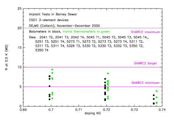
Figure 3 – R(0.5 K) vs. doping for the 19 measured dies.
Table 2 – SHARC II Candidate Wafers from CSO Run 1, with R at 0.5 K
|
Wafer |
R(T1) |
R(T2) |
R(T3) |
R(T4) |
average |
range DR |
|
2041.7200 |
|
5.08 |
6.86 |
|
5.97 |
1.78 |
|
5311.7000 |
|
2.86 |
7.20 |
6.92 |
5.66 |
4.34 |
|
5045.7000 |
1.80 |
2.57 |
5.15 |
7.74 |
4.32 |
5.94 |
|
5251.7200 |
|
|
3.57 |
4.59 |
4.08 |
1.02 |
|
5350.7200 |
|
4.99 |
|
3.08 |
4.04 |
1.91 |
|
5273.7200 |
1.85 |
3.37 |
4.72 |
6.12 |
4.02 |
4.27 |
Resistance
(MW) at 0.5 K of bolometers from
SHARC II candidate wafers. The SHARC II
target is 10 MW.
Wafer
2041 is the best candidate for building SHARC II, with 5311 as a second
choice. It is likely that many elements
from both wafers will have resistances below the SHARC II minimum which was
established earlier in the year.
Therefore, we tabulate below the effects of revising the SHARC II
minimum downward. Assumptions not
stated here are drawn from ‘HAWC and SHARC II Detector Recipe Requirements
Document’, version 4, written by M. Freund.
Q = 75 pW is the original background power estimate; Q = 120 pW is now
considered more likely.
Table 3 –
Effect on Sensitivity of Lowering SHARC II Resistance Requirement
|
|
D = 40 K, R(0.5 K) = 10 MW |
D = 35 K, R(0.5 K) = 5.6 MW |
D = 30 K, R(0.5 K) = 3.0 MW |
|
Q
= 75 pW, f = 0.03 Hz (scanning) |
1.073 |
1.076 |
1.087 |
|
Q
= 75 pW, f = 3 Hz (chopping) |
1.041 |
1.048 |
1.062 |
|
|
|
|
|
|
Q
= 120 pW, f = 0.03 Hz (scanning) |
1.064 |
1.072 |
1.091 |
|
Q
= 120 pW, f = 3 Hz (chopping) |
1.045 |
1.056 |
1.077 |
The
tabulated quantity is NEP(total)/NEP(sky), where NEP(sky) is the fundamental
atmospheric limit.
Table 4 – HAWC Candidate Wafers from CSO Run 1, with R at 0.35 K
|
Wafer |
R(T1) |
R(T2) |
R(T3) |
R(T4) |
average |
range DR |
|
5045.7000 |
7.1 |
10.8 |
26.0 |
43.1 |
21.8 |
36.0 |
|
5273.7200 |
7.4 |
15.2 |
23.3 |
31.4 |
19.3 |
24.0 |
|
5350.7200 |
|
25.0 |
|
13.6 |
19.3 |
11.4 |
|
5251.7200 |
|
|
16.4 |
22.2 |
19.3 |
5.8 |
|
5330.7375 |
|
7.6 |
12.7 |
|
10.2 |
5.1 |
|
5332.7200 |
|
|
6.2 |
|
6.2 |
na |
Resistance
(MW) at 0.35 K of bolometers from
HAWC candidate wafers. The HAWC target
is 13.5 MW.
Thermal
Conductances
If
enough current is applied to the thermistors, the resistance decreases due to
heating. If the thermistor R(T) is
known, the thermal conductance can be derived.
This measurement was performed for the subset of thermistors measured
November 11-14, and the results are reported in the table below. The thermal conductance is modeled as G = G0Tb.
Table 4 –
Measured Thermal Conductances
|
Die |
Substrate
Attachment* |
Thermistor
Type |
G0 nW K-1-b |
b |
G (0.5 K) nW/K |
|
2041.7200
T3 |
direct |
bare
bolometer |
1.62 |
1.98 |
0.41 |
|
5311.7000
T3 |
isolated |
bare
bolometer |
1.91 |
1.95 |
0.49 |
|
|
|
|
|
|
|
|
2041.7200
T3 |
direct |
bolometer w/
Ag |
25.8 |
1.29 |
10.5 |
|
5045.7000
T3 |
direct |
bolometer w/
Ag |
40.9 |
1.36 |
15.9 |
|
5273.7200
T3 |
isolated |
bolometer w/
Ag |
35.8 |
1.18 |
15.8 |
|
5311.7000
T3 |
isolated |
bolometer w/
Ag |
29.6 |
1.36 |
11.6 |
|
5326.7375
T3 |
direct |
bolometer w/
Ag |
65.4 |
1.25 |
27.4 |
|
5330.7375
T3 |
isolated |
bolometer w/
Ag |
49.2 |
1.01 |
24.4 |
|
|
|
|
|
|
|
|
2041.7200
T3 |
direct |
frame |
1510 |
3.71 |
115 |
|
5045.7000
T3 |
direct |
frame |
24900 |
4.63 |
1010 |
|
5273.7200
T3 |
isolated |
frame |
1750 |
4.31 |
88.3 |
|
5311.7000
T3 |
isolated |
frame |
1050 |
3.74 |
78.8 |
|
5326.7375
T3 |
direct |
frame |
8640 |
2.95 |
1120 |
|
5330.7375
T3 |
isolated |
frame |
1900 |
2.68 |
296 |
* Direct: die/GE
varnish/PCB. Isolated: die/GE varnish/perf. board/Stycast/PCB
The
thermal conductance of the bare bolometers is comparable to the design goal (G
= 0.57 nW/K at 0.5 K). The 1000 Å
silver on the back increases the thermal conductance by more than an order of
magnitude. The dies themselves are
heatsunk with a G another order of magnitude higher, as inferred from the frame
thermometers.