Pop-Up Detector Test Report
Version 2.0 -- 25 June 2000
C. Darren Dowell
Caltech, Mail Code 320-47
Pasadena, CA 91125
(626)395-6675 (office)
(626)395-2600 (lab)
(626)796-8806 (FAX)
cdd@submm.caltech.edu
Abstract
Measurements of semiconducting pop-up bolometers were performed at Caltech
in April 2000. We report the resistance vs. temperature and the thermal
characteristics of the measured samples. The desired SHARCII and HAWC
parameters were bracketed with the measured samples, and we make
recommendations for the bolometer designs for the two instruments.
Acknowledgments
Walter Collins (Caltech), Mino Freund (Goddard), Matt Gardner (Caltech), and
Jeff Groseth (Caltech) helped considerably with preparing the test
components and in performing the measurements. Attila Kovacs (Caltech)
wrote the software to solve for bolometer parameters from measured data.
Christine Allen (Goddard) provided the bolometer samples and advice for
handling them. Harvey Moseley (Goddard) provided guidance through the
testing period. This research was funded in part by NSF grant AST 9615025
to the Caltech Submillimeter Observatory.
Outline
- Measurement apparatus
- Bolometer design
- Thermistor screening results
- Results for 5327 G0 test array
- Results for 5347 G0 test array
- Fitted parameters
- White noise
- Time constants
- Results for 5347 thermistor test array
- Measurements of absorbers
- Results for 5347 thermistor test array
- General conclusions
- Recommendation for SHARCII bolometer design
- Recommendation for HAWC bolometer design
- References
Implant and bolometer samples were tested in the SHARCII cryostat, which
contains a 3He refrigerator enclosed in a L4He-cooled
radiation shield. For most measurements, the main L4He reservoir
was pumped down to 1.5 K so that the device substrate reached temperatures as
low as 0.325 K.
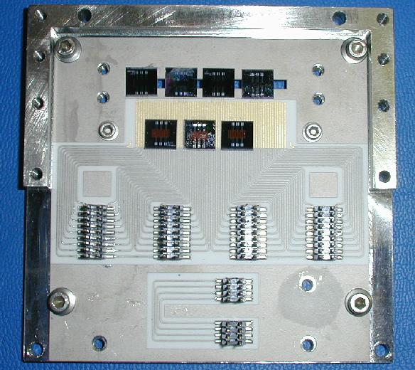
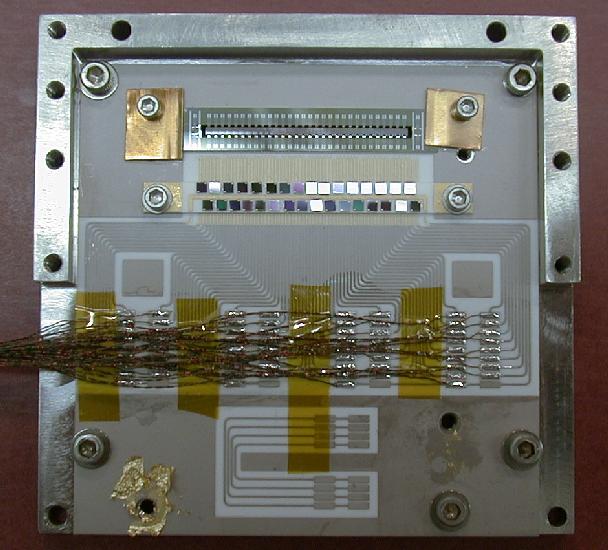
Figure 1. Caltech interface substrate (alumina). The
3-element implant screening devices
were GE varnished to the substrate, and the 32-element bolometer arrays were
clipped to the substrate. Gold wedge bonds provided electrical connection
between the devices, load resistors, and substrate. Surface-mount connectors
were initially
used to interface with the cryostat wiring. However, they were replaced
with directly soldered wires for later measurements. The ceramic substrate
was enclosed in an INVAR box. A sheet of gold leaf and the force
of ~6 screws were used to thermally connect the INVAR and ceramic.

Figure 2. Device suspension and shielding. The ceramic/
INVAR package was suspended from the L4He coldplate with 3-4
fiberglass tubes
with A/L = 0.014-0.018 cm. The package was heat sunk to the fridge through an
annealed OFHC copper strap with A/L = 0.014 cm. A calibrated LakeShore GRT
was attached to the ceramic substrate with a screw and gold leaf, approximately
5 cm from the detectors. The package was shielded by a secondary
L4He
enclosure with blackened walls. With this configuration, the coldest observed
GRT measurement for the detector package was 0.325 K, during which the
L4He bath was at 1.5 K, the fridge was at 0.291 K, and the
extrapolated parasitic heat load on the detector package was 2-4 microW. The
JFET modules were located outside the inner shield.
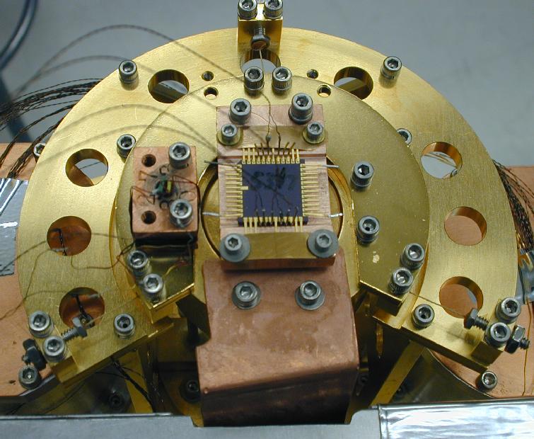
Figure 3. Additional implant screening hardware. In order
to confirm the implant resistances, the 3-element devices in the
Goddard-selected
ceramic package were clipped to a copper block and installed directly
on the SHARC II fridge coldhead or in a separate L4He cryostat
(the purple 'Barney' Dewar).
All wires going into the Dewar pass through one or two RFI-filtered
connectors, which contain 4 nF capacitors from each pin to the Dewar wall.
Thermal Performance of Detector Package
The silicon frame has a thickness of 300 microns. In the direction of heat
flow from bolometer 1 to bolometer 32, the relevant A/L is 0.0035 cm. For
a 0.3 K thermal conductivity of XXX...
The wirebonds were 0.001 inch diameter 99.99% gold. With 64 each 3 mm long
wire bonds (total A/L=0.001 cm), and assuming a 0.3 K thermal conductivity of
0.1 W/cm/K (Touloukian et al. 1970), the effective G of the wirebonds was
100 microW/K. We have ignored unknown boundary thermal resistance, which will
reduce the effective G.
The ceramic substrate is approximately 7 cm x 7 cm x 0.06 cm, giving an
A/L of 800 cm in the thickness (shortest) direction. Assuming a 0.3 K
thermal conductivity of 11 microW/cm/K (Locatelli et al. 1976), the thermal
conductance from the INVAR enclosure to the trace side of the ceramic board is
G = 9000 microW/K. Again, we have ignored boundary thermal resistance.
The heat strap also limits the cooling of the detector wafer. During the
cooldowns reported here, the fridge/heat strap combination was observed to
have an effective G of 80 microW/K at the coldest temperatures.
Combining the effective G's of the wire bonds, ceramic board, and heat
strap, we estimate an effective G of 40 microW/K for the link from the silicon
die to the 3He fridge, three orders of magnitude greater than
the G of the membrane devices.
For a maximum 0.5 V bias across the 64 each 30 Mohm load resistors and
detectors, the
dissipated power can be at most 0.5 microW, leading to a temperature rise of
at most 13 mK. For the 0.5 V bias, the detector package was observed to slowly
warm a few mK. However, the measurements with the 0.5 V bias were performed
quickly, using the thermal inertia of the detector package to keep the
detector cool.
Three types of bolometer arrays were manufactured for the detector measurements:
- 3-element implant screening dies with all membrane (high G) devices
- 32-element G0 variety packs with a range of thermal designs
(HGUNITs)
- 32-element thermistor variety packs with a range of thermistor designs
(THUNITs)
The metallization of the measured wafers was aluminum.
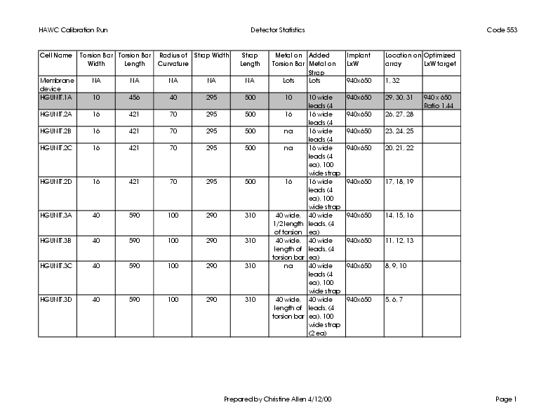
Table 1. Recipes for bolometers on G0 test
arrays.
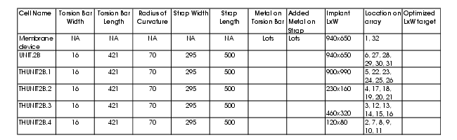
Table 2. Recipes for bolometers on thermistor test arrays.
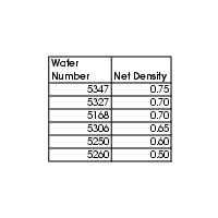
Table 3. Implant doses. Higher net density means greater
implant dose, which means lower cold resistance. Wafers 5347 and 5327 are
of interest for SHARCII and HAWC. (Wafer 5168 was not tested.)
The first part of the detector measurement program was to screen five wafers
for desired resistance at cold temperatures. Three-element membrane devices
were measured in three configurations -- GE varnished to the Caltech ceramic
interface board, packaged in the Goddard ceramic carrier on a copper block
in the purple L4He Dewar, and in the Goddard carrier/copper block
on the SHARCII coldhead.
Resistance measurements were made with a Keithley 616 Digital Electrometer
borrowed from Goddard that allows current excitations from 1 pA to 1 microA
stepped by factors of 10. The reported measurements were made with the
highest current setting which did not cause significant self heating. The
criterion was to allow no more than a 2% effect on the observed resistance.
SHARCII Dewar, Large Ceramic Board
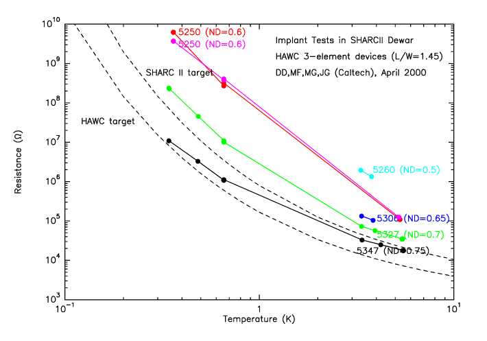
Figure 4. Resistance measurements for 3-element membrane
devices on Caltech ceramic board. The SHARCII target curve is
T0 = 40 K, R0 = 1430 ohm (Moseley et al. 1999),
and the HAWC target is
T0 = 30 K, R0 = 700 ohm (Moseley 1999).
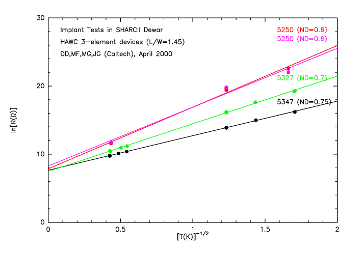
Figure 5. Resistance measurements plotted in units which
give linear fits.
A fit to the data with model
R = R0 exp[(T0/T)1/2] yields:
Label   ND   R0 (ohms)  T0 (K)
-----  ----  ---------  ------
5250a  0.6     2570      81.8
5250b  0.6     3880      74.6
5327   0.7     1750      48.9
5347   0.75    2090      25.7
Table 4. Fits for resistance of implant devices on Caltech
ceramic board.
Purple Dewar, Small Ceramic Package
Three-element dies were tested using the Goddard-provided ceramic packages
attached 'upside down' to a copper block in order to shield the devices
from radiation. Resistances were measured with the Keithley 616 electrometer.
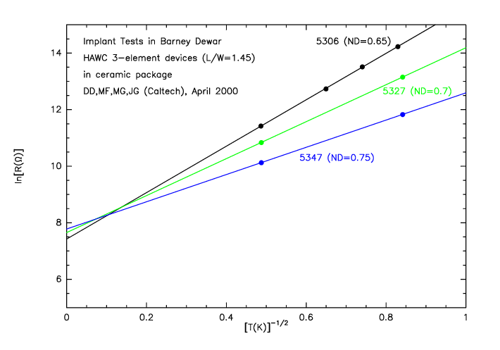
Figure 6. Measurements of thermistor samples in the
purple Dewar.
A fit to the data from the purple Dewar experiment only yields:
Label   ND   R0 (ohms)  T0 (K)
-----  ----  ---------  ------
5306   0.65    1670      67.3
5327   0.7     2100      42.7
5347   0.75    2380      23.2
Table 5. Purple Dewar thermistor fits.
SHARCII Dewar, Small Ceramic Package on Coldhead
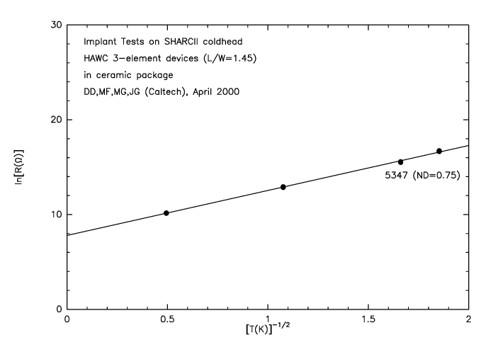
Figure 7. Measurements of thermistor sample on the
SHARC II coldhead. The coldest measured temperature was 0.291 K.
Label   ND   R0 (ohms)  T0 (K)
-----  ----  ---------  ------
5347   0.75    2430      22.5
Table 6. SHARCII coldhead thermistor fit.
Comparison of Samples
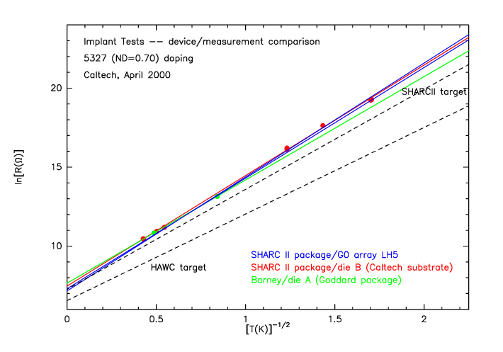
Figure 8. Measurements of 5327 thermistor samples. Two membrane
dies and one 32-element bolometer array were measured. The fits for the
bolometer array represent the extreme values for the array. There is
reasonable agreement among the different samples. The resistance is too
high for both HAWC and SHARCII.
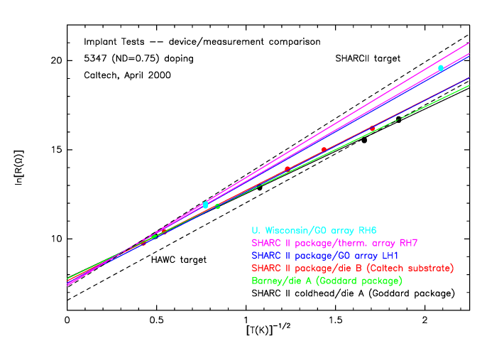
Figure 9. Measurements of 5347 thermistor samples. Two membrane
dies and three 32-element arrays were measured. (The thermistor array
measurements
were normalized to L/W = 1.45.) There is considerable variation from
sample to sample, which nearly covers the range from the HAWC target to the
SHARC II target. There is good agreement between the measurements for
membrane die A in the purple Dewar (green curve) and SHARC II (black curve).
For tests of G0 array 5327 LH5 (ND=0.7), the silicon frame was
clipped to the detector board with beryllium-copper clips and gold wedge bonded.
Bolometers 17-29 and 32 were wired in series with 150 Mohm SiCr load
resistors from MSI. The resistance of a SiCr load varies with
temperature (up to 210 Mohms at 0.33 K); this effect was measured for a
few resistors and modeled for all of them in the analysis.
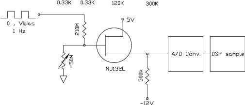
Figure 10. Circuit used to measure IV curves. 16 JFETs
were available, so up to 16 bolometers were measured simultaneously. The
JFET gain was approximately 0.996. The bias voltage was slowly stepped
from 0 V to a nonzero value. The change in voltage from the JFET gives
the bolometer voltage, which yields the bolometer resistance since the
load resistance is known (to 5% accuracy).
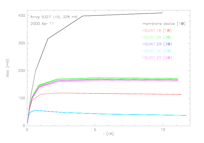
Figure 11. Sample IV curves for all bolometers at a
single temperature.
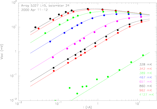
Figure 12. IV curves for a bolometer at multiple
temperatures. The filled circles are measured data, and the lines are
model fits with 4 free parameters.
The bolometer parameters are derived from a minimization procedure in which
the measured I's and V's are compared with a best-fit four-parameter model.
The model is:
- R = R0 exp[(T0/T)1/2]
- G = G0 Tbeta
See Mather (1982) for further details of the model.
G0 test array 5327 LH5
Data at 328, 342, 389, 467, 651, 860, 962, 4127 mK
Negative data included; 4127 mK duplicated
Updated 1 May 2000, 16:30 PDT

R = R0 exp(sqrt(T0/T))
G = G0 T^beta

                        R*     R
          R0    T0    0.3 K  0.5 K   G0=G(1 K)          G(0.3 K)*  G(0.5 K)
bol/grp  ohms    K    Mohms  Mohms  W/K^(beta+1)  beta     W/K       W/K
-------  ----  -----  -----  -----  ------------  ----  ---------  ---------
17 HG2D  1195  51.45   582    30.4    62.3 e-9    2.85   2.02 e-9   8.64 e-9
18 HG2D  1222  51.62   608    31.6    61.9 e-9    2.84   2.03 e-9   8.65 e-9
19 HG2D  1289  50.52   557    29.9    59.0 e-9    2.70   2.29 e-9   9.08 e-9
20 HG2C  1481  48.99   525    29.5     1.56e-9    1.18   0.38 e-9   0.69 e-9
21 HG2C  1321  50.76   589    31.4     1.66e-9    1.31   0.34 e-9   0.67 e-9
22 HG2C  1316  50.67   580    31.0     1.68e-9    1.31   0.35 e-9   0.68 e-9
23 HG2B  1412  49.70   549    30.2     1.61e-9    1.25   0.36 e-9   0.68 e-9
24 HG2B  1474  49.36   549    30.4     1.57e-9    1.23   0.36 e-9   0.67 e-9
25 HG2B  1363  50.43   582    31.3     1.62e-9    1.30   0.34 e-9   0.66 e-9
26 HG2A  1277  51.60   634    33.0    59.9 e-9    2.81   2.03 e-9   8.54 e-9
27 HG2A  1358  51.20   640    33.7    57.5 e-9    2.74   2.12 e-9   8.61 e-9
28 HG2A  1336  50.88   605    32.1    58.8 e-9    2.71   2.25 e-9   8.99 e-9
29 HG1A  1290  51.96   670    34.5    24.2 e-9    2.63   1.02 e-9   3.91 e-9
32  mem. 1299  51.76   658    34.1   202   e-9    2.31  12.5  e-9  40.7  e-9

* extrapolation
Table 7. Four-parameter fits for G0 bolometer
array 5327 LH5.
The fits in Table 7 are somewhat unsatisfactory, as evidenced by the
systematic underestimate of the bolometer resistance at the lowest and
highest temperatures (Figure 12). Better fits are obtained with a slightly
different thermistor behavior, such as
R = R0 exp[(T0/T)0.59]. Alternatively, we
fit just the data at the colder temperatures to achieve better accuracy
there.
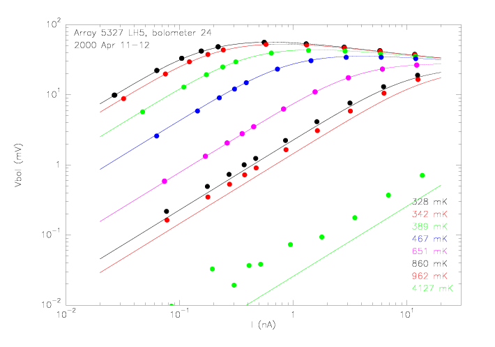
Figure 13. IV curves for bolometer 24, with fit to low
temperature data only (T < 0.8 K).
G0 test array 5327 LH5
Data at 328, 342, 389, 467, 651 mK
Updated 1 May 2000, 16:40 PDT

R = R0 exp(sqrt(T0/T))
G = G0 T^beta
                        R*     R
          R0    T0    0.3 K  0.5 K   G0=G(1 K)          G(0.3 K)*  G(0.5 K)
bol/grp  ohms    K    Mohms  Mohms  W/K^(beta+1)  beta     W/K       W/K
-------  ----  -----  -----  -----  ------------  ----  ---------  ---------
17 HG2D   599  58.28   677    29.3   123   e-9    3.63   1.56 e-9   9.93 e-9
18 HG2D   539  59.68   720    29.9   135   e-9    3.72   1.53 e-9  10.2  e-9
19 HG2D   590  58.26   665    28.8   129   e-9    3.61   1.67 e-9  10.6  e-9
20 HG2C   581  58.39   665    28.7     2.44e-9    1.72   0.31 e-9   0.74 e-9
21 HG2C   580  59.08   721    30.5     2.46e-9    1.78   0.29 e-9   0.72 e-9
22 HG2C   589  58.76   705    30.1     2.47e-9    1.76   0.30 e-9   0.73 e-9
23 HG2B   587  58.51   682    29.3     2.45e-9    1.76   0.29 e-9   0.72 e-9
24 HG2B   597  58.46   689    29.6     2.41e-9    1.75   0.29 e-9   0.72 e-9
25 HG2B   596  58.78   715    30.5     2.40e-9    1.77   0.28 e-9   0.70 e-9
26 HG2A   632  58.62   744    31.9   118   e-9    3.60   1.55 e-9   9.73 e-9
27 HG2A   636  58.80   765    32.6   120   e-9    3.60   1.57 e-9   9.90 e-9
28 HG2A   627  58.44   722    31.1   124   e-9    3.58   1.67 e-9  10.4  e-9
29 HG1A   630  59.22   796    33.6    42.6 e-9    3.30   0.80 e-9   4.33 e-9
32 mem.   650  58.62   765    32.8   610   e-9    3.54   8.60 e-9  52.4  e-9

* extrapolation
Table 8. Four-parameter fits for array 5327 LH5, using
only data at T < 0.8 K.
The fits using only the low temperature data give 0.3 K resistances which
are ~20% higher, 0.5 K resistances which are ~2% lower, 0.3 K G's which are
~25% lower, and 0.5 K G's which are ~15% higher.
The derived values of beta are somewhat surprising. The devices with only
silicon legs have measured beta's of 1.3 - 1.8, while beta's of 3 (the value
expected for a dielectric) were measured in the 12 micron silicon bolometers
(e.g., Wang et al. 1996). The speculation is that the thermal conductance is
dominated by the heavily doped traces, which have a metallic beta of 1
(H. Moseley, private communication).
The devices with metal on the legs, on
the other hand, have steep beta's of 2.7 - 3.6. While normal metals should
give a beta of 1, the aluminum metallization is superconducting at these
temperatures and may have a much more steep beta.
The addition of 100 micron wide metal to the strap has essentially no effect
on the thermal conductance. A bolometer with the design HGUNIT.2D (metal) has
the same G as HGUNIT.2A (no metal), and HGUNIT.2C (metal) has the same G as
HGUNIT.2B (no metal).
All bolometers were wired with 30 Mohm nichrome load resistors from MSI.
The nicrohme resistors are much more temperature stable, and their
resistance is known to 1% accuracy. The full array was measured with two
separate cooldowns between which the routing of the 16 JFETs was changed.
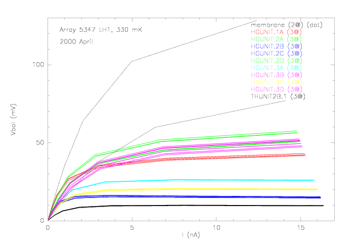
Figure 14. Sample IV curves for all bolometers at a single
temperature.
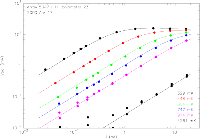
Figure 15. Sample IV curves for a single bolometer at
multiple temperatures.
G0 test array 5347 LH1
Data at 330, 440, 597, 742, 985, 4243 mK (pixels 1-16)
Data at 329, 448, 604, 744, 974, 4261 mK (pixels 17-32)
Updated 1 May 2000, 16:50 PDT

R = R0 exp(sqrt(T0/T))
G = G0 T^beta

                        R*     R
          R0    T0    0.3 K  0.5 K   G0=G(1 K)          G(0.3 K)*  G(0.5 K)
bol/grp  ohms    K    Mohms  Mohms  W/K^(beta+1)  beta     W/K       W/K
-------  ----  -----  -----  -----  ------------  ----  ---------  ---------
01 mem.  1844  26.25   21.3   2.59    23.3 e-9    0.55  12.1  e-9  15.9  e-9
02 TH.1  1290  25.58   13.2   1.65     1.07e-9    1.32   0.22 e-9   0.43 e-9
03 TH.1  1365  25.51   13.8   1.73     1.20e-9    1.19   0.29 e-9   0.53 e-9
04 TH.1  1401  25.31   13.7   1.72     0.94e-9    1.15   0.24 e-9   0.42 e-9
05 HG3D  1953  26.94   25.5   3.01    24.4 e-9    1.97   2.28 e-9   6.23 e-9
06 HG3D  1956  27.16   26.5   3.11    24.1 e-9    1.96   2.28 e-9   6.19 e-9
07 HG3D  2147  27.11   28.9   3.39    19.4 e-9    1.77   2.30 e-9   5.69 e-9
08 HG3C  2127  26.93   27.7   3.27     2.24e-9    1.20   0.53 e-9   0.98 e-9
09 HG3C  1844  27.58   26.9   3.10     2.66e-9    1.38   0.51 e-9   1.02 e-9
10 HG3C  1898  27.05   25.2   2.97     2.61e-9    1.35   0.51 e-9   1.02 e-9
11 HG3B  1934  28.40   32.5   3.63    24.2 e-9    2.03   2.10 e-9   5.93 e-9
12 HG3B  1908  28.51   32.7   3.63    25.1 e-9    2.06   2.10 e-9   6.02 e-9
13 HG3B  1869  28.76   33.4   3.68    27.8 e-9    2.14   2.11 e-9   6.31 e-9
14 HG3A  1840  28.67   32.4   3.58     4.08e-9    1.44   0.72 e-9   1.50 e-9
15 HG3A  1951  28.41   32.9   3.66     3.80e-9    1.42   0.69 e-9   1.42 e-9
16 HG3A  1924  28.37   32.2   3.59     3.89e-9    1.41   0.71 e-9   1.46 e-9
17 HG2D  1893  28.73   33.7   3.71    38.4 e-9    2.63   1.62 e-9   6.20 e-9
18 HG2D  1899  28.90   34.8   3.80    38.7 e-9    2.66   1.57 e-9   6.12 e-9
19 HG2D  1981  28.82   35.8   3.93    36.7 e-9    2.65   1.51 e-9   5.85 e-9
20 HG2C  2025  28.51   34.7   3.85     1.17e-9    1.35   0.23 e-9   0.46 e-9
21 HG2C  1839  28.97   34.1   3.72     1.31e-9    1.43   0.23 e-9   0.49 e-9
22 HG2C  1920  28.91   35.2   3.85     1.26e-9    1.40   0.23 e-9   0.48 e-9
23 HG2B  1957  29.47   39.4   4.22     1.21e-9    1.37   0.23 e-9   0.47 e-9
24 HG2B  2038  29.15   38.9   4.22     1.17e-9    1.34   0.23 e-9   0.46 e-9
25 HG2B  1929  29.84   41.4   4.37     1.25e-9    1.40   0.23 e-9   0.47 e-9
26 HG2A  1871  30.40   44.0   4.55    42.4 e-9    2.76   1.53 e-9   6.26 e-9
27 HG2A  2019  29.93   44.0   4.63    37.3 e-9    2.62   1.59 e-9   6.07 e-9
28 HG2A  1952  30.41   46.0   4.76    40.0 e-9    2.69   1.57 e-9   6.20 e-9
29 HG1A  1836  31.16   49.0   4.92    20.0 e-9    2.74   0.74 e-9   2.99 e-9
30 HG1A  1788  31.95   54.2   5.30    20.7 e-9    2.80   0.71 e-9   2.97 e-9
31 HG1A  1927  31.34   52.9   5.29    18.1 e-9    2.68   0.72 e-9   2.82 e-9
32 mem.  1814  32.12   56.5   5.49    72.9 e-9    1.58  10.9  e-9  24.4  e-9

* extrapolation
Table 9. Four-parameter fits for G0 bolometer
array 5347 LH1.
Although the measured values of G make qualitative sense, the scaling with
leg geometry is not what was expected. This will be discussed further in the
Conclusions.
Resistance Gradient
The cold resistance goes from high at bolometer 32 to low at bolometer 1. In
order to confirm this situation, a few bolometers were measured individually
with an electrometer. The 0.327 K resistance measured in the linear portion
of the IV curve is tabluated below:
           Electrometer  Table 9 Fit
            Resistance   Resistance
Bolometer      Mohm         Mohm
---------  ------------  -----------
    1          15.6         14.4
    9          19           18.0
   12          23           21.7
   15          22           21.8
   24          28           25.7
   32          36.4         36.6
Table 10. Resistance gradient in G0 array 5347 LH1.
A radiation gradient as the cause of the resistance can be ruled out since
the membrane (high G) devices and bolometers (low G) are affected about the
same. WHAT ABOUT A TEMPERATURE GRADIENT???
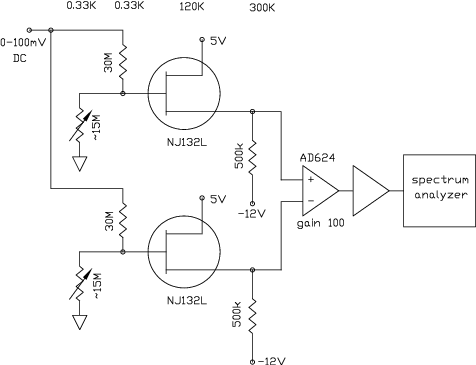
Figure 16. Differential readout used for noise
measurements. The differential readout was the only one available with the
desired bandwidth (lowpass filtering at ~250 Hz), but it has the advantage
of common mode noise rejection of bias fluctuations and microphonics.
Figure 17. Noise spectra for bolometers 22-21 on 5347 G0
array LH1. The bolometers are of type HGUNIT2C. The observed noise has been
divided by the amplifier gain (except the
low pass filtering) and by 21/2 to show the noise for a single
bolometer referred to the JFET input. The 1/f noise in the 40 mV and 157 mV
spectra is most likely due to operation of the JFETs at a non-optimal
temperature. The short horizontal lines at right
show the noise predicted from the IV curve fits in the ~30 Hz region. The
predictions are in good agreement with the observations. The calculated
electrical NEP for the optimal 40 mV bias is 6.1x10⁻¹⁷
W s1/2.
Figure 18. Circuit used for time constant measurements.
For the time constant measurements, the bolometers were driven using a bias
waveform with a square profile switching between two positive levels 8 mV
apart. The output of the JFET was sent to an
SR560 preamplifier with a gain of 100 and then to an oscilloscope. DC coupling
was used on both instruments; a DC level from a power supply was subtracted to
bring the signal on scale. Low-pass filtering was applied with the SR560,
but the cutoff frequency (typically 3 kHz) was chosen so that only high
frequency noise was eliminated and the shape of the waveform was preserved.
Additional filtering of the bolometer waveform was caused by the bias waveform
filtering (cutoff frequency at 6800 Hz) and the RFI connectors (cutoff
frequency at 20 kHz, assuming a 1000 ohm JFET output impedance). These cutoff
frequencies are high enough to be irrelevant.
Figure 19. Typical oscilloscope trace during time constant
measurement. Shown is the output of the JFET for bolometer 24 of the 5347
G0 test array, multiplied by a gain of 100. The bias frequency was
8 Hz, and the settling time was 3.6 msec.
The overshoot is caused by the high-frequency impedance of the bolometer
being larger than the low-frequency impedance (Mather 1982). Stated another
way, the dynamic circuit model of a bolometer contains an effective inductance,
which creates a voltage spike at the transition of the bias.
Our interpretation is that the settling time of the voltage following the bias
transition is the true detector time constant (taue in the
notation of Mather 1982).
For the measured quantities, we looked at the transition caused by the positive
change in the bias. We recorded:
- V(step) -- the voltage from the initial (flat) voltage to the final (flat)
voltage.
- V(o.s.) -- the voltage from the final (flat) voltage to the peak
voltage. ('o.s.' for overshoot.)
- t(o.s.) -- the time from the beginning of the transition to the peak
voltage.
- t(settle) -- the time from the peak to when the voltage has slewed 63%
of the way to the final voltage. The true time constant taue.
In the table below, voltages are referred to JFET output, before the
preamplification. The calculated G and T are the estimates from the IV curve
fits.
                                                     calc.   observ.
            bias  calc G  calc T  V(o.s.)  t(o.s.)  V(step)  V(step)  t(settle)
bol.  grp.   mV    nw/K      K       mV      msec      mV       mV       msec
----  ----  ----  ------  ------  -------  -------  -------  -------  ---------
  9    3C    25     0.59   0.34     0.12     2.2      2.9      2.7       1.5
  9    3C    49*    0.64   0.36     0.42     1.1      1.4      1.4       1.6
  9    3C    98     0.76   0.40     0.70     0.52     0.34     0.40      1.2
  9    3C   196     0.98   0.48     0.61     0.28     0.02     0.06      0.71

 15    3A    39     0.84   0.34     0.19     1.8      2.2      2.2       1.6
 15    3A    78?*   0.95   0.38     2.8?     0.92     0.90     6.6?      1.1
 15    3A   157     1.20   0.44     0.69     0.31     0.12     0.18      0.61
 15    3A   314     1.60   0.54     0.47     0.24    -0.02     0.05      0.31

 18    2D    49     2.1    0.34     N.A.     N.A.     2.7      2.6       0.38
 18    2D    98*    2.5    0.36     0.20     0.8      1.5      1.5       0.68
 18    2D   196     3.6    0.41     0.46     0.31     0.45     0.53      0.36
 18    2D   392     5.6    0.48     0.34     0.22     0.12     0.22      0.16

 24    2B    20     0.28   0.34     0.39     2.4      2.6      2.7       4.5
 24    2B    39*    0.31   0.37     1.1      1.3      1.2      1.1       3.6
 24    2B    78     0.38   0.43     1.2      0.6      0.17     0.11      2.3
 24    2B   157     0.50   0.53     0.74     0.4     -0.03    -0.13      1.3

* optimum bias for NEP
? apparent errors in measurement, probably bias amplitude setting
Table 11. Time constant measurements for G0 array
5347 LH1 operated at 0.328 K.
Fitted Parameters
Thermistor test array 5347 RH7
Data at 330, 451, 610, 755, 971, 4190 mK
Updated 1 May 2000, 16:55 PDT; corrected grp labels 25 June 2000

R = R0 exp(sqrt(T0/T))
G = G0 T^beta

                        R*     R
          R0    T0    0.3 K  0.5 K   G0=G(1 K)          G(0.3 K)*  G(0.5 K)
bol/grp  ohms    K    Mohms  Mohms  W/K^(beta+1)  beta     W/K       W/K
-------  ----  -----  -----  -----  ------------  ----  ---------  ---------
09 TH.4  1622  35.93   91.8   7.79     1.53e-9    1.67   0.20 e-9   0.48 e-9
10 TH.4  1658  35.50   87.9   7.57     1.52e-9    1.64   0.21 e-9   0.49 e-9
11 TH.4  1622  35.65   88.0   7.54     1.54e-9    1.69   0.20 e-9   0.48 e-9
12 TH.3  1800  34.29   79.1   7.11     1.42e-9    1.49   0.24 e-9   0.51 e-9
13 TH.3  1733  34.60   80.0   7.10     1.48e-9    1.53   0.23 e-9   0.51 e-9
14 TH.3  1726  34.57   79.3   7.05     1.49e-9    1.52   0.24 e-9   0.52 e-9
15 TH.3  1800  34.52   82.0   7.31     1.44e-9    1.51   0.23 e-9   0.51 e-9
16 TH.3  1802  34.41   80.7   7.22     1.44e-9    1.50   0.24 e-9   0.51 e-9
17 TH.2  1638  36.36   99.0   8.28     1.50e-9    1.57   0.23 e-9   0.51 e-9
18 TH.2  1668  36.19   98.2   8.26     1.49e-9    1.56   0.23 e-9   0.51 e-9
19 TH.2  1727  36.17  101     8.53     1.43e-9    1.56   0.22 e-9   0.48 e-9
20 TH.2  1693  36.09   98.2   8.29     1.46e-9    1.56   0.22 e-9   0.50 e-9
21 TH.2  1578  36.79  102     8.38     1.55e-9    1.62   0.22 e-9   0.50 e-9
22 TH.1  1096  33.11   40.0   3.75     1.42e-9    1.45   0.25 e-9   0.52 e-9
23 TH.1  1106  33.47   42.8   3.95     1.37e-9    1.42   0.25 e-9   0.51 e-9
24 TH.1  1108  33.03   40.0   3.75     1.37e-9    1.42   0.25 e-9   0.51 e-9

* extrapolation
Table 12. Four-parameter fits for thermistor test array 5347 RH7.
There is no strong resistance gradient across the RH7 thermistor device, as
confirmed by the following 0.330 K measurements with an electrometer:
           Electrometer
            Resistance
Bolometer      Mohm
---------  ------------
    1          42.8
    6          44
   31          44
   32          35.0
Table 13. Electrometer resistance measurements for thermistor test
array 5347 RH7.
Noise -- DC Bias
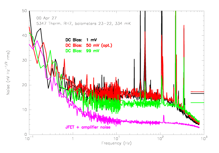
Figure 20. Noise spectra for bolometers 23-22 on 5347 thermistor
test array RH7. The measurement technique and analysis are the same as in
Figures 16 and 17. The bolometers are of type THUNIT2B.1 and have full-area
thermistors. The predictions at right are for 10 Hz.
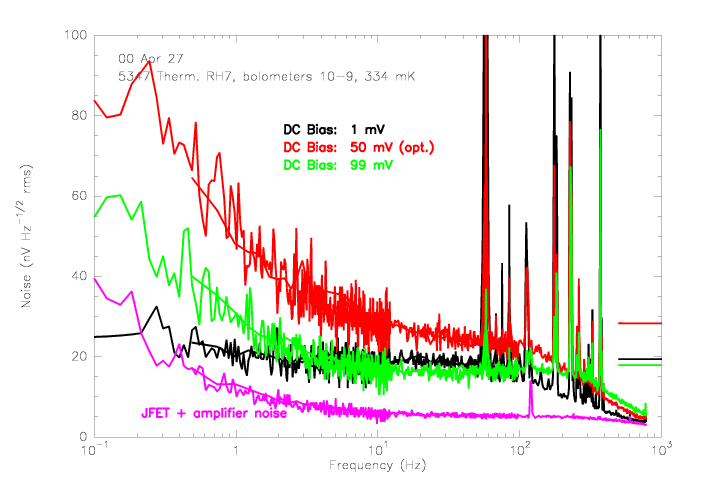
Figure 21. Noise spectra for bolometers 10-9 on 5347 thermistor
test array RH7. The bolometers are of type THUNIT2B.4 and have small
thermistors. The veritical display range has been enlarged by a factor of
2 compared to Figure 20.
Low Frequency Noise (AC Bias)
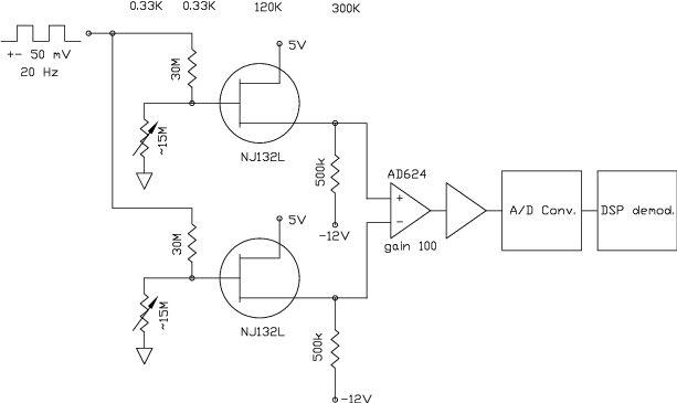
Figure 22. Electronics configuration used to measure low-frequency
noise. The amplifier circuit is the same as in Figure 16. Differences now
are the AC bias on the detector and demodulation (in the DSP) prior to the
Fourier transform (in software).
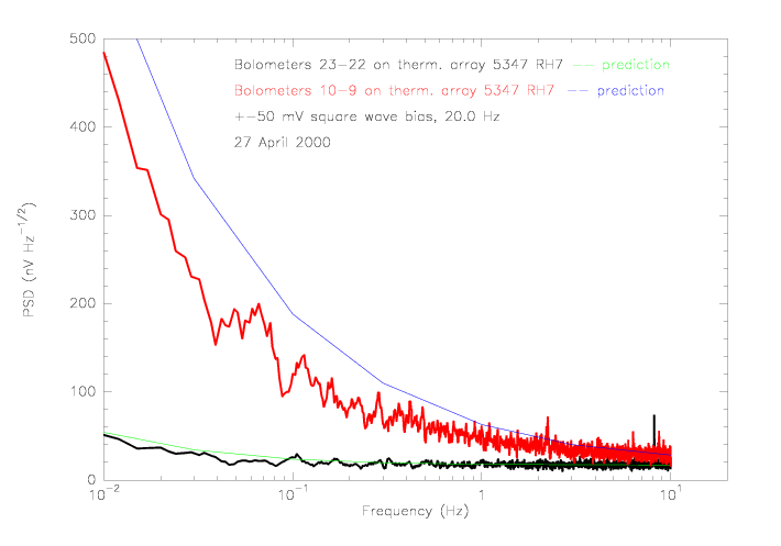
Figure 23. Low-frequency noise spectra for bolometers 23-22 and 10-9
on 5347 thermistor test array RH7. The noise has been divided by
21/2 and corrected for the amplifier gain to express the noise
for a single bolometer. The predictions are based on the IV
curves and the 1/f noise model of Han et al. (1998). For the bolometers with
full-area thermistors, an NEP of 2x10-16 W s1/2
was observed at 0.01 Hz, and 9x10-17 W s1/2 at 0.1 Hz.
Time Constants
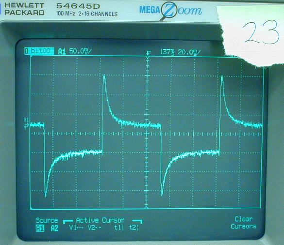
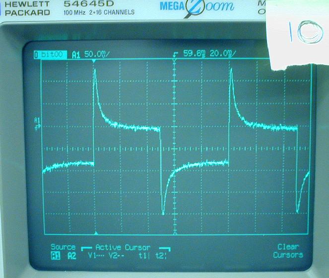
Figure 24. Oscilloscope traces during time constant measurements
of bolometers 23 (full area thermistor) and 10 (small thermistor) from
thermistor test array 5347 RH7. The measurement technique was the same as
in Figure 19. The bias frequency was 10 Hz. The transition times are
similar.
                                                     calc.   observ.
            bias  calc G  calc T  V(o.s.)  t(o.s.)  V(step)  V(step)  t(settle)
bol.  grp.   mV    nw/K      K       mV      msec      mV       mV       msec
----  ----  ----  ------  ------  -------  -------  -------  -------  ---------
 10   TH.4   50*    0.34   0.40     1.3      1.3      0.82     0.80      3.6
 10   TH.4  100     0.47   0.49     1.1      0.36    -0.044   -0.025     2.1
 23   TH.1   50*    0.36   0.39     1.3      1.2      0.73     0.70      4.2
 23   TH.1  100     0.45   0.46     1.1      0.58     0.035    0.019     2.8

* optimum bias for NEP
Table 14. Time constant measurements for thermistor test array
5347 RH7 operated at 0.331 K.
At these temperatures, the size of the thermistor only plays a small role in
the time constant and heat capacity -- 30% at most.
Thermistor array sample 5347 RH7 was returned to Goddard and coated on the
back side with a 175 ohm (room temperature in air) Pd/Au film. The array was
measured cold on June 22-23, 2000 in the same Caltech apparatus as above.
Similarity of Resistance and Thermal Conductance
The observed resistances before and after the absorbers were applied are
essentially the same, indicating that radiation leaks onto the array are
not a significant problem. The thermal conductances are also the same.
         before after  before after    before     after     before      after
           R*     R*     R      R
         0.3 K  0.3 K  0.5 K  0.5 K  G(0.3 K)*  G(0.3 K)*  G(0.5 K)   G(0.5 K)
bol/grp  Mohms  Mohms  Mohms  Mohms     W/K        W/K        W/K       W/K
-------  -----  -----  -----  -----  ---------  ---------  ---------  ---------
19 TH.2  101    115     8.53   8.59   0.22 e-9   0.18 e-9   0.48 e-9   0.49e-9
21 TH.2  102    117     8.38   8.47   0.22 e-9   0.18 e-9   0.50 e-9   0.51e-9
23 TH.1   42.8   46.9   3.95   4.07   0.25 e-9   0.21 e-9   0.51 e-9   0.48e-9
24 TH.1   40.0   43.5   3.75   3.94   0.25 e-9   0.21 e-9   0.51 e-9   0.49e-9
29 2B      NA    80.5    NA    6.44      NA      0.20 e-9      NA      0.55e-9
30 2B      NA    80.0    NA    6.55      NA      0.20 e-9      NA      0.53e-9
32 mem.    NA    68.5    NA    6.00      NA      9.12 e-9      NA     33.2 e-9

* extrapolation
Table 15. Comparison of resistance and thermal conductance
measurements before and after application of Pd/Au absorbing film onto
thermistor test array RH7.
Increased Time Constants
The time constants were 4-5 times higher, indicating a large heat capacity in
the Pd/Au film.
                                   before      after
            bias  calc G  calc T  t(settle)  t(settle)
bol.  grp.   mV    nw/K      K       msec       msec
----  ----  ----  ------  ------  ---------  ---------
 21   TH.2   76     0.44   0.46                  15
 23   TH.1   24     0.32   0.36                  16
 23   TH.1   50     0.36   0.39      4.2         19
 23   TH.1   76     0.42   0.43                  16
 23   TH.1  100     0.45   0.46      2.8         16
 30   2B     76     0.44   0.45                  15
Table 16. Comparison of time constants before and after application
of absorbing film. The 'before' measurements had an operating temperature
of 0.331 K, and the 'after' measurements had an operating temperature of
0.345 K.
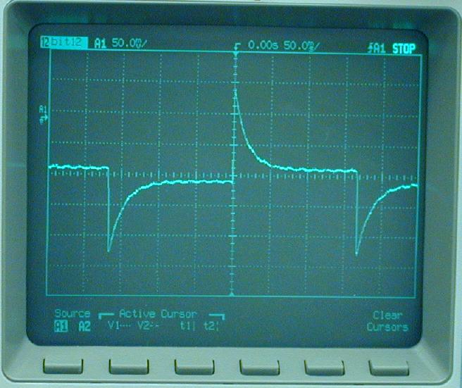
Figure 25. Oscilloscope trace during time constant measurements
of bolometer 23 on thermistor array 5347 with an absorbing film. Compare
with Figure 24, and note the change in horizontal scale (msec/division).
The following conclusions apply to the operating temperatures of the
measurements (0.33 - 1 K):
- Doping of ND = 0.75+-0.05 is suitable for HAWC and SHARCII. However, an
accurate selection of doping is made difficult by the resistance variation
across the 5347 (ND = 0.75) wafer.
- The 5327 (ND = 0.70) wafer had 0.3 K resistances of ~480 Mohms/square and
0.5 K resistances of ~22 Mohms/square.
- The 5347 (ND = 0.75) wafer had 0.3 K resistances of ~32 Mohms/square, but
with a range of 9.7 to 70. The 0.5 K resistances were ~3.1 Mohms/square, with
a range of 1.4 to 5.9.
- Bolometers with no metal on the torsion bars have thermal conductances
with a T1.2 to T1.8 temperature dependence.
- Adding aluminum to the torsion bars significantly increases the thermal
conductances and changes the temperature dependence to
T2.0 to T3.6.
- Adding metal to the strap region has a minimal effect on the thermal
conductance.
- The quantitative behavior of the thermal conductances is discussed below.
- The electrical time constants for the detectors at 0.4 K are
approximately 1 msec for a G of 1 nW/K.
- The heat capacity from large thermistors is not significant compared to
the rest of the pixel. The contribution of a full area thermistor
is ~25% at 0.4 K.
- There is no evidence for excess noise in the bolometers in the white
noise region (a few Hz to ~100 Hz). Electrical NEP's down to
6x10-17 W s1/2 have been observed.
- With a full-area thermistor, the useful bolometer signal band can be
extended down to ~10 mHz, permitting scanning observing modes. The 1/f noise
roughly follows the prediction of Han et al. (1998).
The most perplexing aspect of the detector measurements is the behavior of the
thermal conductances, summarized in the table below:
                                tors. bar    tors. bar  G(0.3 K)*    G(0.5 K)
therm. struct.    wafer/sample  silicon W/L  metal W/L     nW/K         nW/K
----------------  ------------  -----------  ---------  ----------  -----------
HG2B, HG2C, TH2B  5327 G0 LH5      0.038       0        0.28- 0.38   0.66- 0.74
HG2B, HG2C, TH2B  5347 G0 LH1      0.038       0        0.22- 0.29   0.42- 0.53
HG2B, HG2C, TH2B  5347 th RH7      0.038       0        0.20- 0.25   0.48- 0.52

HG3C              5347 G0 LH1      0.068       0        0.51- 0.53   0.98- 1.02

HG3A              5347 G0 LH1      0.068       0.136^   0.69- 0.72   1.41- 1.50

HG1A              5327 G0 LH5      0.022       0.022    0.80- 1.02   3.91- 4.33
HG1A              5347 G0 LH1      0.022       0.022    0.71- 0.74   2.82- 2.99

HG2A, HG2D        5327 G0 LH5      0.038       0.038    1.53- 2.29   8.54-10.6
HG2A, HG2D        5347 G0 LH1      0.038       0.038    1.51- 1.62   5.85- 6.26

HG3B, HG3D        5347 G0 LH1      0.068       0.068    2.10- 2.30   5.69- 6.31

membrane          5327 G0 LH5      large       large    8.60-12.5   40.7 -52.4
membrane          5347 G0 LH1      large       large         10.9         24.4

* extrapolation
^ only on cold half of torsion bar
Table 17. Summary of thermal properties of HGUNIT's and THUNIT's.
As noted in the section "Results for 5327 G0 Test Array LH5", the
G's for metal-free legs go as ~T1.5, and the G's for the metallized
legs go as ~T3. We have offered an explanation for the unexpected
temperature dependence in that section.
The HGUNIT.2B/C, HGUNIT.3C, and HGUNIT.3A devices on 5347 G0 array LH1 can be
used to estimate the dependence of G on torsion bar width and length for
devices with no metal; we calculate a W1.06L-0.45
dependence at 0.3 K and W1.03L-0.53 at 0.5 K.
(We have assumed that the metal half-way up the torsion bar on
HGUNIT.3A is sufficient to cool that part of the bar to the base operating
temperature.) In macroscopic/high temperature situations, we expect
W1 and L-1, so the observed L dependence is surprising.
For the metallized devices (HGUNIT.1A, HGUNIT.2A/D, and HGUNIT.3B/D), the
situation is even more surprising. The range
of torsion bar lengths is not large, so we fit for the dependence of G
on (W/L) together and calculate (W/L)0.99 at 0.3 K and
(W/L)0.64 at 0.5 K, dominated presumably by width dependence. This
is quite far from the expected (W/L)2 dependence.
It is possible that the 0.5 K measurements of the metallized bolometers
especially are contaminated by heating effects in the silicon frame and/or
detector package.
Following is the SHARCII bolometer design recommendation resulting from this
study:
- Full area thermistor (>=900 micron by >=900 micron).
- Target resistance of 10 Mohms at 0.5 K. Acceptable range: 5-20 Mohms.
This resistance will be achieved with ND ~ 0.73 and will result in
T0 ~ 40 K and R0 ~ 1300 ohms/square.
- Thermal design intermediate between HGUNIT.2B and HGUNIT.3C -- a torsion
bar with W ~ 25 micron, L ~ 500 micron, and no metallization. HGUNIT.2B is
also acceptable.
The following table summarizes the expected operating conditions of the
SHARCII bolometers as designed above:
       parameter            value      units
-----------------------  ----------  ---------
operating temperature       0.32         K
T0                         40            K
R0                       1300           ohm
thermistor volume           2.7e-7      cm^3
G0                          1.9      W K^-2.35
beta (G = G0 T^beta)        1.35
R (load resistor)         200           Mohm
T (load resistor)           2.0          K
background power           75            pW
NEP (background)            4.4e-16   W s^1/2
voltage noise (amp.)        5  e-9    V s^1/2

V (bias)                  500            mV
V (bolometer)              19.4          mV
I                           2.4          nA
R (bolometer)               8.1         Mohm
Z (bolometer)               2.8         Mohm
T (bolometer)               0.52         K
G                           0.79        nW/K
S                           1.3e+8      V/W
NEP (detector, 0.01 Hz)     2.8e-16   W s^1/2
NEP (detector, 0.1 Hz)      1.4e-16   W s^1/2
NEP (detector, 1 Hz)        1.2e-16   W s^1/2
NEP (detector, 10 Hz)       1.2e-16   W s^1/2
det. volt. noise, 10 Hz    16  e-9    V s^1/2
time constant (elec.)       1           msec
Table 18. SHARCII bolometer characteristics, updated from Moseley
et al. (1999).
TBD
Han, S.-I., et al. 1998, in EUV, X-Ray, and Gamma-Ray Instrumentation for
Astronomy IX, ed. O. Siegmund & M. Gummin, Proc. SPIE 3445, "Intrinsic 1/f
Noise in Doped Silicon Thermistors for Cryogenic Calorimeters"
Locatelli, M., Arnaud, D., & Routin, M. 1976, *journal unknown*,
"Thermal conductivity of some insulating materials below 1K"
Mather, J. C. 1982, Applied Optics 21, 1125, "Bolometer noise: nonequilibrium
theory"
Moseley, H. 1999, memo dated July 29, "Detector Design for HAWC"
Moseley, S. H, Dowell, C. D., Allen, C, & Phillips, T. G. 1999, in
Imaging at Radio Through Submillimeter Wavelengths, ed. J. Mangum &
S. Radford, ASP Conf. Ser., "Semiconducting Pop-Up Bolometers for
Far-Infrared and Submillimeter Astronomy"
Toloukian, Y. S., Powell, R. W., Ho, C. Y., & Klemens, P. G. 1970, Thermal
Properties of Matter, Volume 1, Thermal Conductivity -- Metallic Elements and
Alloys, IFI/Plenum: New York
Wang, N., et al. 1996, Applied Optics, 35, 6629, "Characterization of a
submillimeter high-angular-resolution camera with a monolithic silicon
bolometer array for the Caltech Submillimeter Observatory"