Measurements of Bismuth Absorber

Darren Dowell -- (626)395-6675 (office), -2600 (lab), 796-8806 (FAX)


Last modified Sunday, 25-Feb-2001 9:51 PST
cdd@submm.caltech.edu

SHARC II absorber, cold DC resistance -- February 2001

Cold electrical resistance measurements of witness samples prepared and measured by Christine Allen (GSFC) are shown below:
R vs. T of witness samples
R vs. cycle

SHARC II absorber, FTS characterization -- February 2001

Christine Allen (GSFC) deposited 154 Angstroms bismuth and 175 Angstroms SiO on a silicon wafer provided by Mino Freund (GSFC). Ken Stewart (GSFC) measured the cold transmission of the coated wafer as well as an uncoated one on February 23, 2001. The transmission spectra were modeled using the equations of Clarke et al. (1977).
spectrum of bare wafer
Figure 1. Cold transmission spectrum of bare wafer. The red curve shows the best 'by-eye' fit to the data (black dots) using the index of refraction of silicon (n = 3.38) from Loewenstein et al. (1973). The green curve shows the index of refraction (n=3.28) which best fits the transmission minima. In both cases, an absorption of 1% was found. The wafer thickness (101.5 and 104.6 microns) was treated as a free parameter and was fit using the fringe spacing.

spectrum of coated wafer
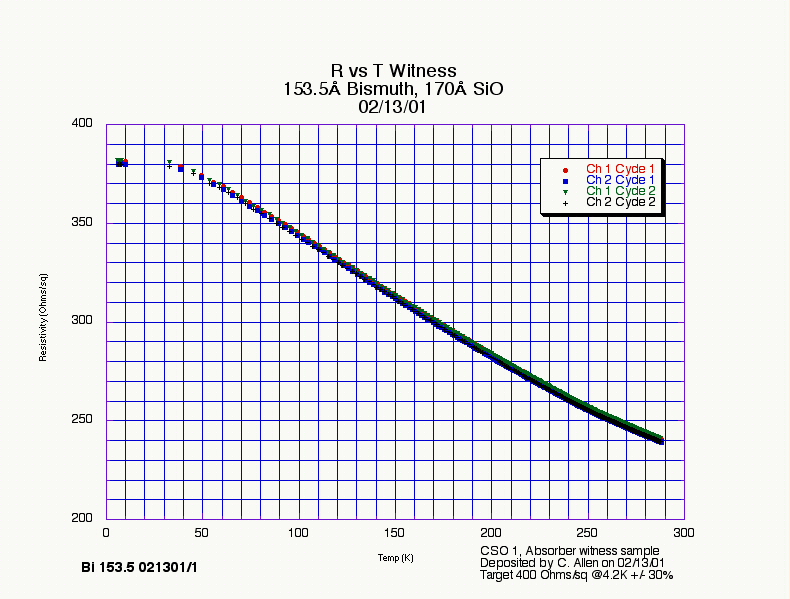
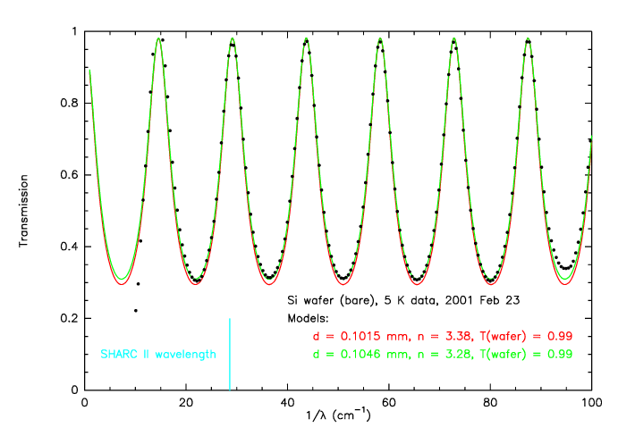
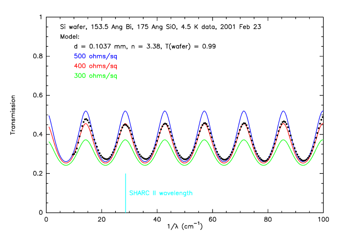
Figure 2. Cold transmission spectrum of coated wafer. For the models, the Loewenstein et al. (1973) index of refraction for silicon is used, and the silicon absorption (1%) is the same as in Figure 1. The green, blue, and red curves show the predictions for 300, 400, and 500 ohms/square. The resistance which best fits the data (black dots) is approximately 430 ohms/square. The wafer thickness was fit to be 103.7 microns.

spectrum of coated wafer
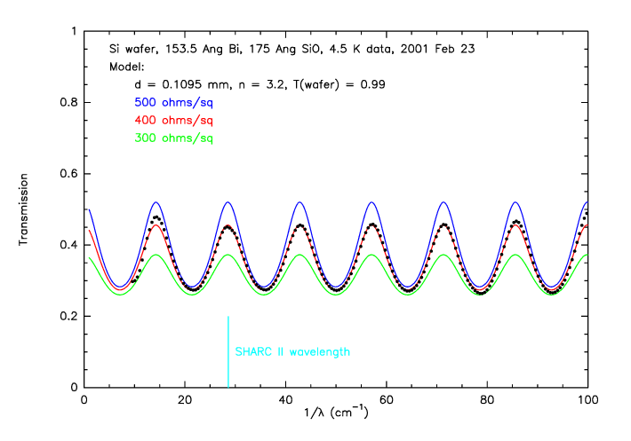
Figure 3. Cold transmission spectrum of coated wafer. For these models, the index of refraction (n = 3.2) was optimized to best fit the fringes. The silicon absorption (1%) is the same as in Figure 1. The green, blue, and red curves show the predictions for 300, 400, and 500 ohms/square. The resistance which best fits the data (black dots) is approximately 400 ohms/square. The wafer thickness was fit to be 109.5 microns.

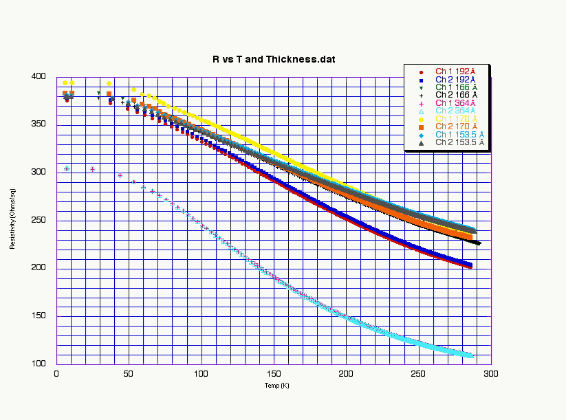
CONCLUSION: This bismuth deposition recipe produces 400 ohms/square DC (electrical) on the witness sample and 400 ohms/square in the far-IR (optical) on the FTS sample wafer. The SHARC II target resistance is 400 ohms. THEREFORE, THE FIRST SHARC II BOLOMETER DEPOSITIONS SHOULD USE THIS ABSORBER RECIPE.


Go to SHARC II home page...