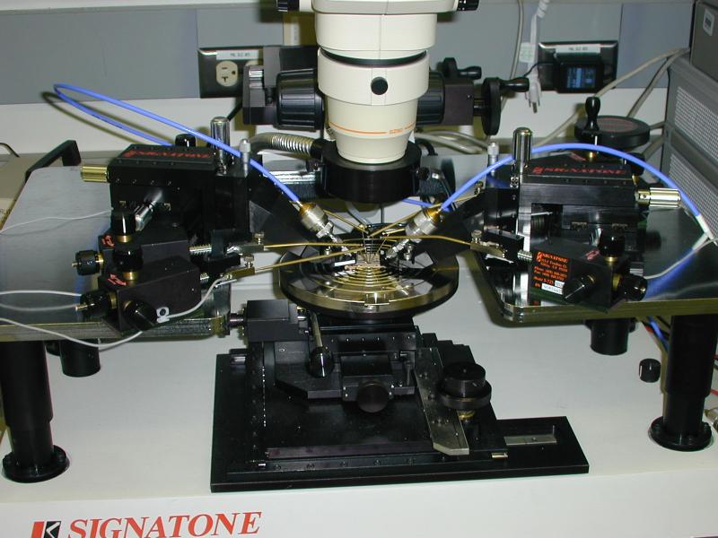
Testing the QMMIC on a Probe Station

Warnings
WARNING:
It is extremely easy to destroy the QMMIC while probing. Bumping any of the
capacitors or air bridges will destroy the chip.
WARNING:
It is vitally important that the QMMIC be kept in a safe place until the
probe station is completely set up and ready to go.
WARNING:
Practice probing a dead chip before taking a good chip out of the drawer.
WARNING:
Don't try to pick up the chip with bent or dirty tweezers. The chip will
slip out of the tweezers and get scratched or lost or otherwise broken.
WARNING:
Don't bump the probes, probe station, or table top while the chip is being
probed.
WARNING:
Be sure to examine all probe tips and test all the positioners before
taking out the chip. In particular, make sure that the positioners
move smoothly without catching or jerking. If they do not move smoothly,
fix them before taking the chip out of the drawer!
Detailed Instructions
-
Make sure the QMMIC chip is safely put away in a Lista drawer. Don't
get it out until the probe station is completely ready!
-
Inspect the probe positioners carefully. Move all screws to
approximately their center positions. Make sure the motion is
smooth.
-
Install the 150 micron microwave probes. Inspect the DC probe
needles, and replace any that have excessively bent or dull tips.
Then install the DC probes.
-
Position the DC probes tips to be reasonably close to where
they will need to be. Make sure that they are close enough that
the last little bit can be adjusted entirely with the micro
positioners. Make sure that the positioners will have enough downward
travel left to contact the chip.
-
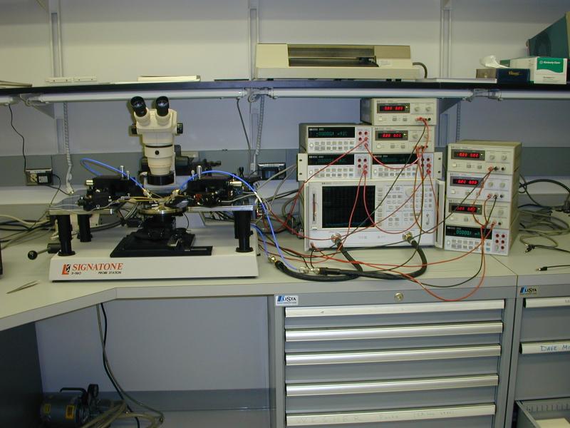
Hook up the bias supplies. The grounds can be connected through
the network analyzer. You will need
- 3 power supplies for the drains, from 0 to 3 Volts
- 3 current meters for the drains, to read from 0 to 10 mA
- 3 power supplies for the gates, from -3 to 0 Volts
-
Set all bias voltages to 0. Double check the connections. Make
sure none of the probes is shorted to anything. Check each supply
to make sure no current flows for non-zero voltages.
-
Calibrate the network analyzer. The test power should be set to about
-40 dBm. Test the cal to make sure it looks good. Get a blank floppy
disk ready to store data.
-
Find a good pair of tweezers. Make sure the tips aren't bent. Clean
the tips carefully with acetone.
-
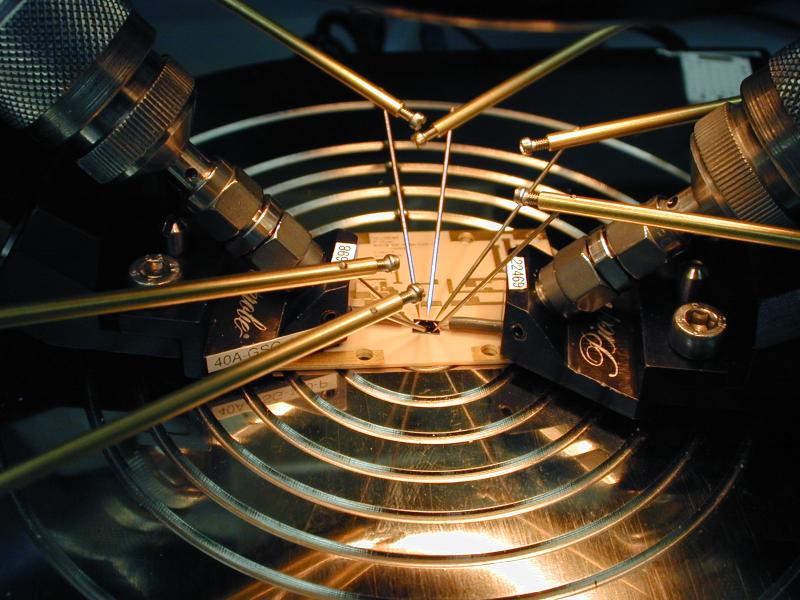
Place a dead MMIC chip on a piece of circuit board. Put the circuit
board on the probe station. Position the microwave probes just above
the CPW pads, but do not contact them yet. Very carefully position
the DC probes just above the DC bias probes, but don't contact them yet.
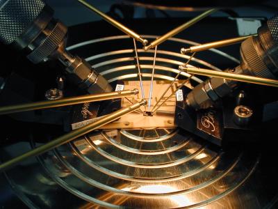
-
Only after all probe tips are correctly positioned just above the
pads, contact the microwave probe tips, then the DC probe tips.
-
Now that you have gotten some practice with the dead chip, and gotten
all the probes perfectly lined up, carefully raise the DC probes about
a millimeter, one at a time, then raise the RF probes. Put away the
dead chip and replace it with a good chip. Lower and contact the RF
probe tips as before, then contact the DC probe tips.
-
Turn the drain voltages up to 0.5 V. There should be a little
bit of current on the drains, very roughly about 1 mA. Turn
the voltages up to about 1.0 V. Then check each gate, one at
a time. Turning a gate voltage up by minus a few tenths of a
volt should decrease the corresponding drain current. If it
doesn't, turn the gate voltage back to zero and check all wiring,
inspect the probe positioning under the microscope, etc. until the
problem has been fixed.
-
By now, S21 should have some gain on the network analyzer.
Adjust the drain and gate voltages as desired. Try to not let the
drain current get larger than 6 or 7 mA, as there is no reason to do so.
-
As soon as testing is finished and all data has been stored, turn
all the bias supplies to 0. Carefully raise each DC probe one at
a time, being extremely careful to not scratch the chip. Then raise
the microwave probes. Put the chip away before doing anything else.
Understanding the Measured Results
The results may have undesirable features such as gain and reflection peaks.
These may be related to substrate modes and/or grounding problems. These
features may change or go away when the chip is mounted in a housing, and
can usually be reduced by adequately grounding both sides of the mounted
chip with several wire bonds.
It should also be noted that the transconductances (and thus the gain)
will increase dramatically as the chip is cooled.