The layers of the QMMIC mask are shown in the table below. The substrate is gold-backed 250 micron GaAs. The circuit has no via holes to simplify fabrication.
| QMMIC Layers | |
| Material | Thickness |
| Gold Bump Metal | 8 microns |
| Bridge Gold | 1 micron |
| Air Bridge Base | 2 microns |
| SiN Dielectric (epsilon = 6.7, 296 pF / mm2) | 2,000 Angstroms |
| Gold | 1 micron |
| Ni:Cr (80:20) Resistors (50 Ohms/square) | 300 Angstroms |
| GaAs Substrate | 250 microns |
| Gold Backing | 1 micron |
The layout is shown below. The input is coplanar waveguide (CPW) at the left edge of the chip. From left to right, the signal passes through a large DC blocking capacitor, is biased from above by a long, thin resistor, passes through a spiral inductor, and ends in a bump pad for the transistor gate. The transistor sources are grounded through long, thin lines above and below the transistor to add some stabilizing negative feedback. The output of the drain continues to the right through an inductive transmission line, and is biased from below by a wide resistor at the DC blocking capacitor. This pattern repeats three times, ending in the CPW output at the right. Resistive elements just before the output bond pads are used to improve the output match.
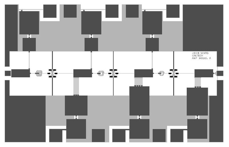
The top half of the chip has an RC filter network for each gate, ending in a bond pad after a voltage divider. By dropping the gate bias voltages by a factor of 10, the dividers both protect the transistors and reduce the effects of noise on the bias lines. The bottom half of the circuit has RC filter networks for the drain bias. Resistors are relatively small to minimize power consumption.
All bond pads have a double thickness of gold. Ground bond areas were added all around the chip. In later testing, it was found that good grounding all around the chip was important to limit substrate modes.
The actual size is about 2.5x3.8 mm.